Modern radar signal processing has become the key to the realization of radar function. According to the system requirements of a radar signal processor, this paper systematically optimizes its hardware structure and software design. A set of four TS201 and one FPGA as the core signal processing board is designed. The system realizes space-time two-dimensional signal processing with only one sub-board. The algorithm of adaptive sidelobe cancellation, 4-way pulse compression and MTI/MTD, sidelobe shadowing and differential beam angle measurement can be used to calculate the target distance and azimuth deviation to meet the system requirements.
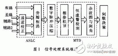
1 System composition analysisThe echo signal is partially combined with the microwave on the antenna to form a sum and difference channel signal and two auxiliary antenna signals for IQ orthogonal interpolation. After 1/8 extraction, 4 channels of data to be tested are formed, and the data rate is 128 MB/ s. The system algorithm structure, as shown in Figure 1, is mainly composed of a sidelobe cancellation module, a digital pulse pressure module, and an MTD processing module consisting of three parts. After the sum signal MTD (FFT-CFAR), the azimuth deviation is calculated from the sum and difference data if the target is determined.

Taking the low-frequency mode of radar operation as an example, the IQ data is 5 388 points and the re-frequency is 140 Hz. Considering a certain amount of time margin, the transmission and processing of 4 signals must be completed in 6.7 ms. . Therefore, the system's data rate, data volume and scale of operation determine that the system design must have the following characteristics:
(1) With high-performance floating-point processing chip, it can complete sidelobe cancellation, pulse compression, coherent accumulation, clutter map, and constant false alarm processing.
(2) High-speed data transfer between internal processing chips and external expansion of the memory chip can save a large amount of data.
(3) It has external data interface and control interface, and can output fault detection signals.
(4) A large number of optimizations must be made in the software design to ensure that all of the above processing modules are completed in one pulse period.
2 radar processor implementation2.1 Hardware platform design
The system operation amount and time requirement, the signal processing board needs to adopt multi-DSP parallel processing structure. In order to achieve high-speed floating-point processing capability, high data throughput rate and large memory space requirements, the DSP chip selects ADSP-TS201, which is the latest ADI company. Model TIgerSHARC architecture high performance floating point digital signal processor. It has an operating clock of up to 600 MHz and can execute up to 4 instructions per cycle; including dual independent arithmetic blocks and dual independent integer ALUs for address calculations, fully parallelizable; with 24 MB/s of on-chip memory Large memory capacity; in addition, 14 DMA controllers and external ports, 4 link ports for high-speed data throughput; 4 SDRAM controllers for external expansion of memory chips; 4 programmable flag pins , can output the desired flag signal to the outside.
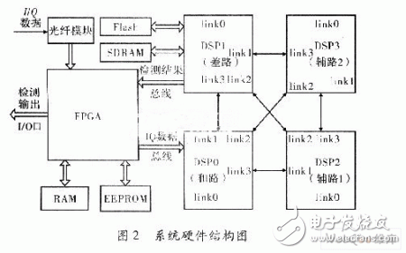
Multi-DSP designs usually have two modes: shared bus mode and link port coupling. The advantage of the shared bus structure is that it can provide a global address space, and map the address space of multiple DSPs to the memory space of the host for unified access. Any DSP can also read and write other processor memory through the bus, which is convenient to operate. However, when data exchange between multiple DSPs is frequent, bus competition often causes a bus bottleneck for data communication, and thus this method has obvious disadvantages. The link port coupling method has obvious advantages. Each DSP bus is independent and has completely independent memory space. Each DSP program design can be completely independent, which reduces the difficulty of program debugging. The DSPs are seamlessly connected only through the link ports, and the number of inter-chip connections is small, which reduces the difficulty and number of layers of the PCB, and saves the cost of the board. In addition, the DMA mode of data transmission using the link port does not occupy the computing time of the DSP core, which can improve the real-time performance of the processing board. Therefore, four ADSP-TS201s are interconnected through the link ports to form a loosely coupled multi-DSP structure, as shown in FIG. Each DSP can transmit data up to 500 MB/s between any two DSPs through the link port.

The board mainly uses 4 TS201 and 1 FPGA as the core, plus FLASH, SDRAM and fiber and its configuration chip cooperate to complete data storage and transmission. The FPGA mainly completes the timing control matched with the radar in the system, and the data transmission outside the board and the bus communication to the DSP. The FPGA is connected to DSP0 and DSP1 through two independent 32-bit external data buses. It uses a pipeline protocol. The external bus operates at 50 MHz and can achieve a data transfer speed of 400 MB/s, which meets the requirements for high-speed data transmission. . The system clock is 50 MHz, the TS201 operates at 600 MHz at 12 times, and the system's peak processing capacity of the single board can reach 14.4 Gflops. The board operation speed meets the system requirements.
2.2 System software design and optimization
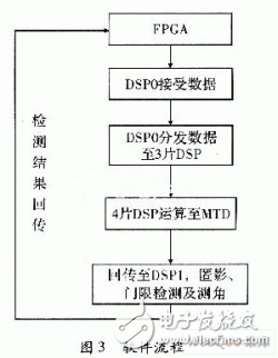
The complexity of the system algorithm and the dynamic range requirements in the calculation, the system algorithm is software-designed in the DSP, and the debugging is convenient. After the echo is synthesized by microwave, the signals of the sum, the difference and the two auxiliary channels are formed. After the A/D samples the orthogonal difference, 4 channels of data are formed into the FPGA through the optical fiber, and DSP0 receives 4 channels of data via the bus and distributes it. To the other 3 DSPs. Each DSP separately processes one channel of data, as shown in Figure 2. After MTD, it is transmitted back to DSP1 for sidelobe and threshold detection, and the target azimuth deviation is estimated. The detection result is returned to FPGA by DSP1 via DMA. The module limit is completed in one pulse period, forming the software flow diagram of Figure 3.

(1) Digital pulse compression.
Electric Junction Box,Waterproof Junction Box,Junction Box Wiring,Pvc Junction Box
CIXI MEMBRANE SWITCH FACTORY , https://www.cnjunma.com
