The NAND gate acts as a switching inverter device and can be used to construct various pulse waveform generating circuits. The basic working principle of the circuit is to utilize the charge and discharge of the capacitor. When the input voltage reaches the threshold voltage VT of the NAND gate, the output state of the gate changes. Therefore, the pulse waveform parameters of the circuit output are directly dependent on the value of the RC component in the circuit.
1, asymmetric multivibrator
As shown in Figure 12-1, NOT gate 3 is used to output waveform shaping.
The output waveform of the asymmetric multivibrator is asymmetrical. When using TTL NAND gates, the output pulse width
Tw1â•RC tw2â•1.2RC Tâ•2.2RC
Adjusting the R and C values ​​can change the oscillation frequency of the output signal. Usually, the C is used to achieve the coarse adjustment of the output frequency, and the potentiometer R is changed to achieve the fine adjustment of the output frequency.

2. Symmetric multivibrator
As shown in Figure 12-2, since the circuit is completely symmetrical, the charge and discharge time constants of the capacitor are the same, so the output is a symmetrical square wave. Changing the values ​​of R and C can change the output oscillation frequency. Non-gate 3 is used for output waveform shaping.
Generally take R≤1KΩΩ, when R=1KΩ, C=100pf~100μf, f=nHz~nMHz, pulse width tw1=tw2=0.7RC, T=1.4RC
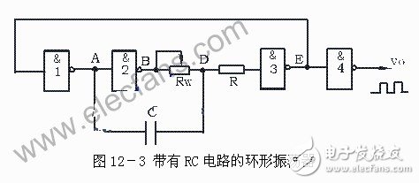
3. Ring oscillator with RC circuit
The circuit is shown in Figure 12-3, the non-gate 4 is used for output waveform shaping, R is the current limiting resistor, generally takes 100Ω, the potentiometer Rw requires ≤1KΩ, the circuit uses the charge and discharge process of the capacitor C to control the voltage D of the D point, Thereby controlling the automatic opening and closing of the NAND gate to form a multi-resonant oscillating, the charging time tw1 of the capacitor C, the discharging time tw2 and the total oscillation period T are respectively
Tw1≈0.94RC, tw2≈1.26RC, T ≈2.2RC
Adjusting the size of R and C changes the oscillation frequency of the circuit output.

The state transitions of these circuits occur at the moment when the NAND gate input level reaches the threshold level VT of the gate. The charging and discharging speed of the capacitor near VT has been slow, and the VT itself is not stable enough, and is susceptible to factors such as temperature, power supply voltage variation, and interference. Therefore, the stability of the circuit output frequency is poor.
4, quartz crystal frequency stabilization multivibrator
When the operating frequency stability of the multivibrator is required to be high, the accuracy of the above several multivibrators cannot meet the requirements. Quartz crystals are commonly used as a reference for signal frequencies. A multivibrator composed of a quartz crystal and a gate circuit is commonly used to provide a clock signal for a microcomputer or the like.
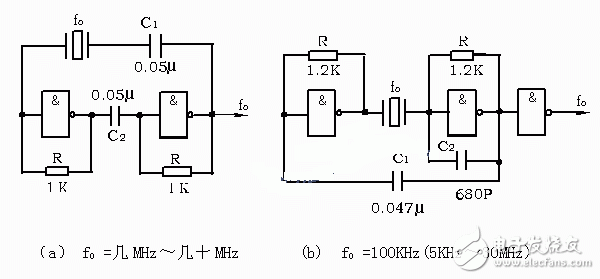
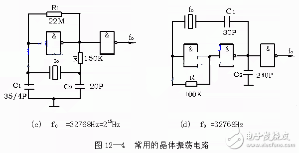
Figure 12-4 shows a typical crystal frequency-stabilized multivibrator.

(a), (b) is a crystal oscillation circuit composed of TTL devices;
(c), (d) is a crystal oscillation circuit composed of CMOS devices, and is generally used in an electronic watch in which f0 = 32768 Hz of the crystal.
In Figure 12-4(c), gate 1 is used for oscillation and gate 2 is used for buffer shaping. Rf is a feedback resistor, usually chosen between tens of megaohms, typically 22MΩ. R acts as a stable oscillator, usually taking ten to several hundred kilohms. C1 is a frequency trimmer capacitor and C2 is used for temperature characteristic correction.

1. Master the basic method of using the gate circuit to form the pulse signal generating circuit
2. Master the calculation method of the timing component value that affects the output pulse waveform parameters.
3. Learning the principle of quartz crystal frequency stabilization and the method of using quartz crystal to form an oscillator
Third, experimental equipment and devices1, +5V DC power supply
2. Double trace oscilloscope
3, digital frequency meter
4, 74LS00 (or CC4011) crystal oscillator 32768Hz potentiometer, resistors, capacitors.
Fourth, the experimental content1. Use the NAND gate 74LS00 to form a multivibrator according to Figure 12-1, where R is a 10KΩ potentiometer and C is 0.01μf.
(1) Observe the output waveform and the voltage waveform across the capacitor C with an oscilloscope, and record it in the list.
(2) Adjust the potentiometer to observe the change of the output waveform and measure the upper and lower limit frequencies.
(3) Use a 100μf capacitor to bridge the 74LS00 near the 14th and 7th feet to observe the loss.
The change of the waveform and the change of the ripple signal on the power supply are recorded.
2. Connect with 74LS00 according to Figure 12-2, take R=1KΩ, C=0.047μf, observe the output waveform with an oscilloscope, and record it.
3. Connect with 74LS00 according to Figure 12-3. The timing resistor RW is connected in series with a potentiometer of 510Ω and a 1KΩ, taking R=100Ω and C=0.1uf.
(1) When RW is adjusted to the maximum, observe and record the waveforms of voltages at points A, B, D, E, and v0, and measure
The period T of v0 and the negative pulse width (charging time of capacitor C) are compared with theoretical calculations.
(2) Change the RW value and observe the change of the output signal v0 waveform.
4. Connect according to Figure 12-4(c). The crystal oscillator is selected from the crystal oscillator 32768Hz, the NAND gate is CC4011, the oscilloscope is used to observe the output waveform, and the frequency meter is used to measure the output signal frequency.
V. Experimental preparation requirements1. Review the working principle of the self-excited multivibrator
2, draw a detailed experimental circuit diagram for the experiment
3. Prepare records, experimental data forms, etc.
Sixth, the experimental report1. Draw the experimental circuit and compare the experimental data with the theoretical values.
2. Draw the working waveforms observed in the experiment with squared paper and analyze the experimental results.
Shenzhen Innovative Cloud Computer Co., Ltd , https://www.xcypc.com
