1 Introduction
Based on the test results, this paper presents the insights into the competitive risks of TTL signals from 10 Hz to 1 MHz.
2 competitive adventure test
2.1 Competitive adventure concept
In digital circuits, if there is a time delay [1] between the input signals, the output may have an interference pulse [1-2]. When the amplitude of the interference pulse reaches the opening level, it will cause harm to the latter circuit and the sensitive circuit. Comparing time delays to competition, interference pulses are like adventures, the so-called "competitive adventures." The core of competitive risk is the interference pulse. The essence of studying competitive risk is to study the interference pulse.
2.2 Test circuit
After testing and comparing various logic circuits, the interference pulse can be generated at the rising edge and the falling edge of the pulse signal at the same time, and the XOR gate is outstanding. Taking the XOR gate 74LS86 chip as an example, a 7-stage XOR gate competitive adventure test circuit is designed.
XOR operation expression: Z = AB+AB, the input is the same (0 0,1 1), the output is 0; if the input is different (0 1,1 0), the output is 1. If the A and H terminals are connected to the TTL digital signal source, the B to G terminals are connected to the 1 state, and the input and output of the odd gate A7 are analyzed. The initial state of the signal source is assumed to be 0, that is, H is 0, Z6 is 0, A7 input is 0 0, then Z7 is 0; assuming 1, that is, H is 1, Z6 is 1, and A7 input is 1 1, then Z7 is still Is 0. After analysis: When A and H are connected to the source, and B to G are all 1 state, the input of A7 is either 0 0 or 1 and Z7 is 0. Since H and Z 6 are delayed signals (there is a time delay between the two signals), the Z7 oscilloscope will display a horizontal bright line with interference pulses.
2.3 Test methods
The test of competitive risk is mainly the test of time delay t and interference pulse amplitude Vp-p [1, 3]. In order to fully understand the interference pulse, this paper also tests the interference pulse width (referred to as the dry pulse width) tp and the interference pulse 10 state position (referred to as the dry pulse state) Vp1/Vp0.
(1) Connect the A and H terminals to the 100 kHz TTL signal, and the B to G terminals to the 1 state. The oscilloscope probes Y1 and Y2 are respectively connected to the H and Z6 terminals, and the oscilloscope is repeatedly adjusted to capture the test object, and the time delay t is measured, that is, the rising edge is t≈75ns, and the falling edge is t≈90ns.
(2) Maintain (1) test conditions and methods, only change the probe Y2 to Z7, and measure the interference pulse amplitude V pp . That is, the rising edge is Vp-p ≈ 2.9V, and the falling edge is Vp-p ≈ 2.6V.
(3) Integrate H, Z6, and Z 7 into a complete rising edge and falling edge competitive risk waveform (see Figure 4). tp, Vp1/ Vp0 parameters are shown in the figure.
3 Conditions for the production of competitive risks
3.1 Interference pulse generation process
On the rising edge: when the first arrival H rises from 0→1, Vp-p≈1.9V is 1 state, and Z 6 is also rising (about 0.6V) but still 0 state, H and Z6 are different. Or change Z7 from 0 to 1; when Z6 is also increased from 0→1, Vp-p ≈3.3V is 1 state, at this time, H and Z6 are all 1 state, and their XOR makes Z7 1 To 0, so the interference pulse is generated instantaneously on the horizontal line of Z7.
The time delay is t≈75ns, the interference pulse amplitude is Vp-p≈2.9V, the dry pulse width is tp ≈80ns, the dry pulse state Vp1 is at the vertical line where H rises by about 1.9V, and the Vp0 position rises by about 3.3V at Z6. Vertical line. According to the dry pulse width tp, another dry pulse state Vp0 position is known.
On the falling edge: the first arrival of H, from 1 → 0 transition, Vp-p ≈ 3.8V is 0 state, at this time Z6 is also falling (about 1.2V) but still 1 state, H, Z6 Or change Z7 from 0 to 1; when Z6 is also decreased from 1→0, Vp-p≈4.0V is 0 state, at this time, H and Z 6 are all 0 states, and their XOR makes Z7 from 1 Back to 0, so the Z7's horizontal bright line also produces an interference pulse. The time delay is t≈90ns, the interference pulse amplitude is Vp-p≈2.6V, the dry pulse width is tp≈70ns, the dry pulse state Vp1 is at the vertical line where H drops by about 3.8V, and the Vp0 position is decreased by about 4.0V at Z6. Vertical line. According to the dry pulse width tp, the position of another dry pulse state Vp0 is known.
On the rising and falling edges, the amplitude of the interference pulse varies. Due to the presence and influence of noise such as line capacitance and inductance, the interference pulse is an asymmetrical waveform, which shows that the rise time is slow and the rise time is steep and the overshoot phenomenon occurs.
3.2 Competitive risk conditions
As can be seen from Figure 4, the generation of competitive risk is constrained by four factors, namely time delay, transition time, logical relationship and delayed signal phase. Time delay [1], that is, the signal is affected by the path, device and other factors in the transmission, the time difference between the input signals [2]; the transition time, that is, the pulse signal state does not change, must undergo a very short transition Time [2]; logical relationship, that is, the logical function formula [4]; the phase of the delayed signal, that is, the phase relationship between the states of the delayed signals, covering both the phase of the delayed signal and the opposite phase of the delayed signal. The same change in the state of the delayed signal is that the delayed signal is in phase, and vice versa. H, Z6 are the same phase of the delayed signal, and the interference pulse is generated in the XOR logic. If H and Z6 are the opposite phases of the delayed signal, even the XOR logic will not generate the interference pulse.
When the signal is transmitted, the time delay phenomenon exists at any time, and the interference pulse sometimes does not exist. The reason is that the logical relationship and the phase element of the delayed signal play a key role. The interference pulse is generated during the transition of the state change signal. Therefore, the time delay and transition time elements are the causes of competitive risk [2]. The logical relationship and the delayed signal phase element are the mechanisms for competing risk. Reasons and mechanisms constitute the conditions for the creation of competitive risks. When the circuit satisfies the generation condition, an interference pulse must be generated.
4 Evolution of competitive risk
4.1 Competitive adventure test of different path and frequency signals
The circuit of Figure 1 is expanded from 7th to 11th (the circuit diagram is omitted), and the generation and evolution of the odd-numbered gates can be explored through longer paths and different frequency signals. See the test parameters of the table.
Table 1 shows the time delay t, the interference pulse amplitude Vp-p, and the interference of the odd-numbered gate signals on the rising edge (£) and the falling edge (£) of the 11-bit XOR gate circuit at 10 Hz to 1 MHz TTL signal. Test parameters for pulse width tp and dry pulse state V p1/Vp0. For the competitive adventure of signals above 1MHz, it is intended to be studied separately. The shaded parts in Table 1 are the test parameters in the "2 Competitive Adventure Test".
4.2 The relationship between competitive risk and signal frequency and transmission path
The output of each odd gate is almost the same at 10 Hz to 1 MHz, indicating that the competitive risk is independent of the signal frequency. As the increase in odd gates is also increasing, it indicates that the generation of competitive risk is related to the signal transmission path, that is, related to the time delay.
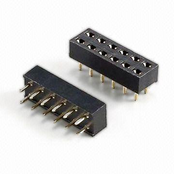
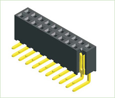
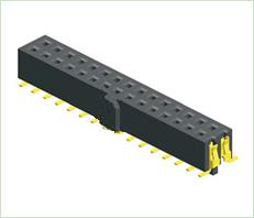
1.ANTENK FEMALE HEADER Series Receptacle Strips are a series of sockets offered in a multitude of sizes and profiles designed to satisfy most .100" pitch socket requirements. Available in Single, Dual and Triple row, they are offered in Straight, Right Angle, SMT, Bottom Entry and Pass Through PCB mounting styles. Each type has a specially designed contact system which uses a wiping mating action and produces a high normal force connection with gold, tin or selective gold plating. All are available with Standard or Hi-Temp Thermoplastic insulators. Our SMT offering is available with optional pick and place pads and tape & reel packaging.
2.Our products are widely used in electronic equipments,such as monitors ,electronic instruments,computer motherboards,program-controlled switchboards,LED,digital cameras,MP4 players,a variety of removable storage disks,cordless telephones,walkie-talkies,mobile phones,digital home appliances and electronic toys,high-speed train,aviation,communication station,Military and so on


2.54 Famale pin headers
SPECIFICATION
Current Rating: 3.0 Amp
Insulation Resistance: 1000M ohms min
Contact Resistance: 20M ohms max
Dielectric Withstanding: AC500V
Operating Temperature: -65°C to +125°C
Contact Material: Brass
Insulator Material: PBT,UL 94V-0 Black
Female Pin Headers,Pcb Female Connectors,Pin Connector Header,Oem Female Header
ShenZhen Antenk Electronics Co,Ltd , https://www.antenk.com
