Switching speed is a complex parameter involving multiple events, each with its own duration. With the patented pHEMT technology, M/A-COM Technology SoluTIons (hereafter referred to as M/A-COM) has found a way to shorten one of the events - the set-up time of the switch - to give Systems such as packet communication networks and radar systems that require strict control of time domain parameters have brought good news. This technology is used in a range of switches from 10MHz to 20GHz, with setup times as short as 20ns.
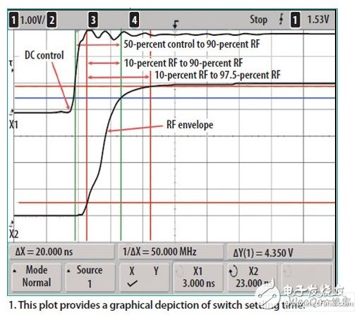
Switching speed and settling TIme, or gate lag, are used to describe high-speed switching performance, but these two parameters are different and often misunderstood. Switching speed is the time it takes for the RF envelope to change from 10% to 90% when the control signal changes the switch from "off" to "on" (Figure 1). The time from the control signal value reaching 50% to the time when the RF envelope reaches 90% is traditionally labeled ton. The rise time required for the RF envelope to change from 10% to 90% is labeled trise. When the control signal changes the switch from "on" to "off", the time from when the control signal reaches its 50% to when the RF envelope drops from 90% to 10% is toff. The separate time for the RF envelope to fall from 90% to 10% is tfall. Gate hysteresis defines the settling time characteristic of the switch after 90% of the RF envelope or 10%.

Figure 1: Graphical illustration of switch setup time.
Unfortunately, the last 10% of the switch transition time can cause a misunderstanding of the traditional switch speed specification because the last 10% is different from the previous 90% change rate. Historically, the response was logarithmic, and the last 10% took time to approach the entire setup time. Normally, for a switch that requires 10 ns to reach 90%, it can take hundreds of milliseconds to reach 100%. This long setup time (gate hysteresis) can cause problems for many systems.
According to the existing apparatus and method, the gate delay of the device can be calculated by measuring the power of the device from 90% to a value set later, such as 97.5% or 100%. In addition, it can also be measured by observing the impedance changes at two fixed time points after the control signal is changed, because the switching device is in a low impedance state in the "on" state and a high impedance state in the "off" state. For example, the gate hysteresis of a device can be described as a 0.5 ohm change in impedance between 10 μs and 10 ms after the control signal changes. Although gate hysteresis cannot be eliminated, M/A-COM Technology SoluTIons has developed a solution for delay due to gate hysteresis.
Whether viewed as a delay or switching impedance change, switches are essential in many test applications and other systems. Some complex packet-based modulation schemes rely on fast transmit/receive or diversity switches to optimize data throughput and reduce signal-to-noise ratio. If the switch is still in the set period when the first packet has been transmitted through it, the envelope shape may be rounded, potentially damaging the data. For high data rate communication applications, fast setup performance can significantly reduce latency before launch. The amount of available data transfer time is equivalent to an increase in throughput.
Setting a short time switch can also bring thermal management benefits. When RF power is applied to a device that is not fully set up, power consumption increases significantly until the device reaches a steady state. Faster setup speeds mean lower power consumption due to series resistance before setup, and lower operating junction temperatures at high power.
The switching delay is primarily related to changing the static charge stored in the active device, the associated circuit, and the time-dependent charge/discharge attenuation effect. There are several factors that cause hysteresis, which can be described by impedance and capacitive reactance. The field effect transistor (FET) has a small gate size and a certain loss. In order to isolate the DC and RF, most of the switch designs usually use a large resistance gate resistor. The gate resistance becomes a factor in determining the resistance constant (RC) time constant. For any change in state (as a first order approximation), the device channel must be depleted or restored, and the electric field around the gate must be created or cleared.
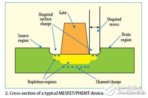
At the device level, reference is made to the simplified cross-section of GaAs MESFET/pHEMT to understand the switching speed and any associated gate hysteresis (Figure 2). The RF switching time is dominated by the charge in the channel region, and the charge is located in the gated and non-gate controlled recess regions near the gate. The on-time of the device is the time required to transfer charge from the source to the drain through the channel after the control signal is applied. The on-time is a function of the corresponding delay time required to fill the channel region with charge. The charge includes channel charge associated with gate capacitance and surface trap charge within the non-gate controlled recess. The turn-off time definition is reversed, and the device will be completely turned off only if the charge in the channel and recess regions is completely removed.

The device cross-section can also visually recognize the relatively fast trise (the time it takes for the RF envelope to rise from 10% to 90%), the time tfall required for the RF envelope to fall from 90% to 10%, and RF The relatively long gate lag time required for the envelope to transition from 90% to 100%. The channel charge associated with the depletion region directly below the gate occupies a major portion of this portion of the charge. By applying the correct pole bias to the gate terminal, charge can be moved into and out of the gate region relatively quickly. On the other hand, the charge in the non-gate-controlled recess is concentrated in the form of surface states and interface traps, which are relatively insensitive to the applied bias voltage and can only pass through a RC circuit formed by a Schottky diode. Discharge. The filling and removal of these surface charges is a slow process that directly leads to an extended gate hysteresis switching time.

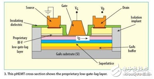
Figure 3: pHEMT profile of a patented low gate hysteresis layer.
What are the advantages of Explosion-proof Screen Protectors?
What is an Explosion-proof Screen Protector? This is a Soft Film made of imported PET material. It has very good flexibility and can help you solve the problems of tilting, white edges, and not suitable for curved screens. Can closely fit the curved edge of the screen.
The PET Screen Protector is made of imported materials from Korea. It is equipped with a proprietary "self-healing" function that can automatically repair minor scratches on the film. Daily protection measures to prevent accidental knocks and drops. The screen strengthens the screen and reduces the chance of cracking. Broken tempered glass is no longer replaced frequently.
1. Edge coverage: The Explosion-proof Screen Protective Film is made of PET flexible material, which is very suitable for the screen of your device, and 100% provides excellent edge coverage, and there is no gap between the edges of the device
2. High-definition resolution: high-definition display, true display of the original screen color.
3. Original touch experience: The oleophobic coating surface of the screen protector can provide your phone with original texture and perfect touch screen response speed. The Soft Film also has oleophobicity and water resistance, which can prevent unnecessary fingerprints.
4. Self-repairing scratches: The Screen Protection Film with self-repairing function can automatically repair tiny scratches and bubbles within 24 hours.
5. Anti-seismic and explosion-proof: PET material has high strength, flexibility and elasticity, which can fully decompose the impact force and prevent the mobile phone from breaking
Explosion-Proof Matte Protective Film,Matte Explosion-Proof Screen Protector,Anti-Scratch Matte Film,Anti-Impact Matte Film
Shenzhen TUOLI Electronic Technology Co., Ltd. , https://www.hydrogelprotector.com
