
In FPGA design, the reset acts as a sync signal that sets all of the storage elements to a known state. In digital circuit design, designers typically implement global reset as an external pin to initialize the design at power up. The global reset pin is similar to any other input pin and is often asynchronous to the FPGA. Designers can use this signal to asynchronously or synchronously reset their designs within the FPGA.
But with the help of tips and tricks, designers can find a more suitable reset structure. An ideal reset structure improves device utilization, timing, and power consumption levels in the FPGA.
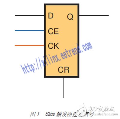
Understanding Trigger Reset Behavior Before delving into the reset technique, it is necessary to understand the trigger behavior within the FPGA slice. Each slice of an FPGA device based on the Xilinx 7 Series architecture contains eight registers, all of which are D-type flip-flops. These triggers share a common control set.
The trigger control set consists of a clock input (CLK), an active-high chip enable (CE), and an active-high SR port. The SR port in the trigger can be used both as a synchronous set/reset port and as an asynchronous preset/clear port (see Figure 1).
Inferring the trigger's RTL code can also infer the type of reset the trigger is ready to use. When the reset signal appears in the sensitive list of the RTL process, the code infers an asynchronous reset (as shown in Figure 2a). The synthesis tool then infers a trigger whose SR port is configured to preset or clear the port (represented by the FDCE or FDPE trigger primitive). After the SR port is asserted, the output of the trigger is immediately forced to the SRVAL attribute of the trigger.
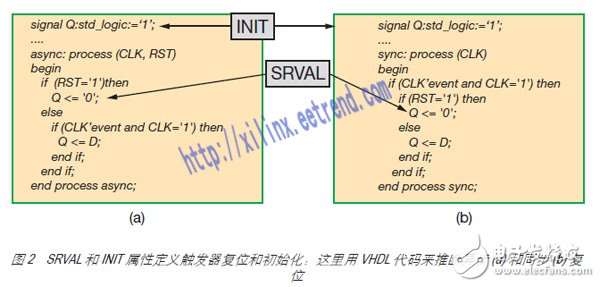
In the case of a synchronous reset, the synthesis tool infers that the SR port is configured to set or reset the port (represented by the FDSE or FDRE trigger primitive). After the SR port is asserted, the output of the flip-flop will be forced to the SRVAL attribute of the trigger on the next rising edge of the clock cycle.
In addition, you can initialize the output of the trigger to the value specified by the INIT attribute. During the configuration process, when the global set/reset (GSR) signal is asserted, the INIT value is loaded into the trigger.
Triggers in Xilinx FPGAs support both asynchronous and synchronous reset and set control. However, the underlying trigger can only implement one setup/reset/preset/clear at a time. If you encode multiple settings/reset/preset/clear conditions in the RTL code, one of the implementations will use the SR port of the trigger, and the rest will use the architectural logic and will take up more FPGA resources.
If one of the conditions is synchronous and the other is asynchronous, the implementation of the asynchronous state will use the SR port and the implementation of the synchronization state will use the architectural logic. In general, try to avoid more than one setup/reset/preset/clear condition. In addition, for each trigger group in Slice (four triggers are a group), there is only one attribute that determines whether the SR port of the trigger is synchronous or asynchronous.
Reset method Regardless of which type of reset (synchronous or asynchronous) is used, it is generally necessary to synchronize the reset with the clock. As long as the global reset pulse is long enough, all flip-flops on the device will go into a reset state. However, the assertion to cancel the reset signal must meet the timing requirements of the flip-flop to ensure that the flip-flop transitions smoothly from the reset state to the normal state. If the timing requirements are not met, the trigger will enter a metastable state.
In addition, for the normal operation of certain subsystems, such as state machines and counters, all flip-flops must exit the reset on the same clock edge. If different parts of the state machine exit the reset state at different clock cycles, the state machine may enter an illegal state. This requires that the cancellation of the reset assertion must be synchronized with the clock.
For designs that use the synchronous reset method in a given clock domain, using a standard metastable solution circuit (two back-to-back flip-flops) is sufficient to synchronize the global reset pin to a specific clock domain. This synchronous reset signal can initialize all of the memory elements in the clock domain using the synchronous SR port on the flip-flop. Since the synchronizer and flip-flop to be reset are all in the same clock domain, the standard PERIOD constraint for this clock domain includes the path timing between the synchronizer and the flip-flop. Each clock domain in the device requires a separate synchronizer to generate a synchronized global reset for that clock domain.
Now go to the real part. Here are some specific tips and tricks to help you find the best design reset strategy.
Tip 1: When driving the trigger's synchronous SR port, each clock domain requires a local version of the global reset and is synchronized with the clock domain .
Sometimes there is no guarantee that a part of the design has a valid clock. This situation usually occurs in systems where the clock used by the system is the recovered clock, or the clock used by the system is derived from the hot-swap module. In this case, it may be necessary to initialize the storage elements in the design by asynchronous reset using the asynchronous SR port on the trigger. Even if the storage element is using an asynchronous SR port, the cancellation of the reset edge assertion must still be synchronized with the clock. This requirement is mainly reflected in the reset of the flip-flop to restore the timing arc, which is similar to the requirement to set the deassertion edge of the asynchronous SR to be synchronized with the rising edge of the clock. If the requirements of this timing arc are not met, the trigger will enter the metastable state and the synchronization subsystem will enter the abnormal state.
Car Screen Protector,Car Center Console Screen Protector,Car Touchscreen Screen Protector
Shenzhen Jianjiantong Technology Co., Ltd. , https://www.jjtscreenprotector.com