
300 MHz internal clock rate
FSK, BPSK, PSK, Linear FM, AM Operation
Two integrated 12-bit digital-to-analog converters (DACs)
Ultra High Speed ​​Comparator, RMS Jitter: 3 ps
Excellent dynamic performance: 80 dB SFDR (100 MHz ± 1 MHz AOUT)
4× to 20× Programmable Reference Clock Multiplier
Two 48-bit programmable frequency registers
Two 14-Bit Programmable Phase Offset Registers
12-bit programmable amplitude modulation and switching output shape keying
Single Pin FSK and BPSK Data Interfaces
PSK functionality via input/output interface
Linear or non-linear FM linear frequency modulation with single-pin frequency hold
AD9854 circuit diagramThe following gives an easy way to develop a high-precision frequency signal generator using the AD9854. The developer only needs to be familiar with MCS-51 microcontroller programming. The system has the characteristics of short development cycle and low development cost. It can also be used as a method to explore the function of AD9854. Its circuit schematic is shown in Figure 2.
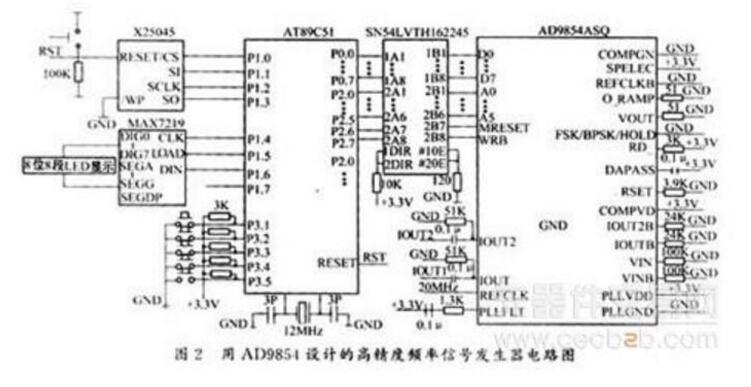
The system consists of DDS chip AD9854, single-chip AT89C51, watchdog timer X25045 and LED display driver chip MAX7219. An 8-bit seven-segment LED display is provided in this system. The first five bits are the output frequency values. The display range is 00.000 to 99.999 MHz. The last three bits are the amplitude display bits. The display range is 0 to 999, indicating that the amplitude is zero. The rate of change to full range.
Realization of AD9854 Control by 16-bit MCUThe single-chip microcomputer used to control the AD9854 is Sunplus SPCE061A. It is a 16-bit microprocessor with a clock frequency of 0.32MHz-49.152MHz, 32K words of flash memory, and 2K words of working static memory. There are 32-bit I/O ports, which are divided into 16-bit IOA ports and 16-bit IOB ports. Each port can be individually configured for input and output. But this one-chip computer does not have the read-write timing control pin of other one-chip computers, so in controlling to AD9854, need to come up with a pin separately as the read-write timing pin.
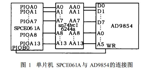
As shown in Figure 1, to control it, we must first set up its external circuit, according to our experimental requirements, the REFCLKB pin connected to the power supply, the implementation of single-ended input mode. Then set the S/PSE2LECT pin to 1 and use the parallel input/output method.
After the external circuit is set up, the I/O update signal of the AD9854 is set. Whether the signal control is correct depends on whether the AD9854 can work normally. The I/O update signal is a low-to-high rising edge generated by transferring operation input data from the I/O buffer register to the DDS core register. This signal can be provided externally or internally. When this signal is provided externally, we should set the INT/EXTUpdateClk bit in the control register to 0. At this time, the internal system clock will be synchronized with it to prevent transfer of the data portion of the program register and cause program execution errors. To generate this internally, set the INT/EXTUpdateClk bit to 1. The default I/O Update signal has a period of 65×(SYS2TEMCLOCKPERIOD×2). The same internally generated I/O update signal can also be controlled by the 32-bit UpdatedClock register (addresses 16-19). The signal cycle equation is (N+1)×(SYSTEMCLOCKPERIOD×2), where SYS2TEMCLOCKPERIOD is 1/SYSTEMCLOCK,N It is the value that needs to be input to the 32-bit register, and its range of application is 1 to (232-1). The duration of the high level of the I/O Update signal is 8 clock cycles.
Next, set the internal 40 registers in the AD9854. Among them, the register with the address 1D-20 is a 32-bit control register, which controls the operating mode, comparator, output amplitude, and system clock.
First, set the register with address 1D. This register controls the comparator switch and the switching of each output path. In the experiment, no comparator was used, and each channel was required to have output. Therefore, the 1D address control register keeps the default value of 10h.
Register 1E controls the on-chip PLL multiplier switch and multiplier multiplier. In the experiment, external 20MHz crystal oscillator is used as the oscillation source for the AD9854, and the system operating clock is set to 200MHz. Therefore, the PLLRange bit in the 1E register is set to 1, due to the use of the AD9854's internal PLL multiplier. So the Bypass PLL bit is set to 0 and the multiplier multiplier should be set to 10, so the contents of the 1E address controller should be 4Ah.
The control register with the address 1F mainly controls the operating mode of the chip and the internal and external modes of I/O update. We still use the single-tone mode, and also use internally generated I/O update signals. Therefore, the register uses the default value 01h.
The control register at address 20 is mainly the control of the amplitude of the output waveform and some settings during serial input and output. In the experiment, we used the parallel input and output methods, so some of the serial settings default to 0. For the amplitude setting, if the internal amplitude of the AD9854 is to be generated, the OSKEN bit is set to 0 and the OSKINT bit is set to 1. If the output amplitude is regulated by a special amplitude register, the OSKEN bit is set to 1 and the OSKINT bit is set to 0. In the experiment, the content of this control register is still set to the default value of 20h, and the output amplitude is adjusted by a special amplitude register.
After setting the control register, we set the frequency register, amplitude register, and phase register again. There are two frequency registers and two phase registers in the chip. Since we use the Single-Tone mode, we only use the PhaseAdjust1 and FrequencyTuningWord1 registers.
The PhaseAdjust register controls the phase of the generated waveform at addresses 00 and 01. It is a 14-bit register and thus the resulting waveform has a 14-bit phase.
The FrequencyTuningWord register controls the frequency of the waveform. The address is from 04 to 09. Its precision is 48 bits. Therefore, we need to input the 48-bit frequency control word. The formula for the frequency control word is: FTW=(DesiredOutputFrequency×2N). )/SYSCLK. Where N is the resolution of the phase accumulator, we take 48 here, and the calculated frequency control word is a decimal number, so it should be converted into a 48-bit binary number. The frequency range controlled by this register can range from 0 to 1/2 SYSCLK. SYSCLK is the chip's system clock.
The registers that control the amplitude are OutputShapeKeyI and OutputShapeKeyQ with addresses 21 through 24, both of which are 12-bit registers.
In the AD9854 read and write operations, the important issue is to pay attention to its read and write timing, in the experiment, we did not read the AD9854 operation, so the following only describes the write operation timing.
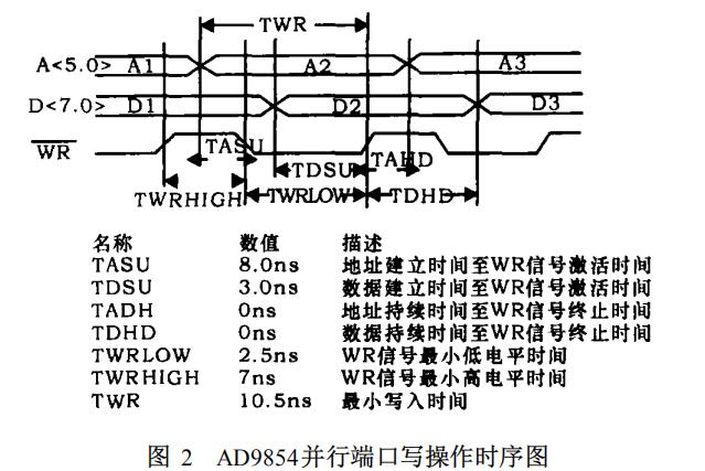
As shown in Fig. 2, the address and data can be written at the same time when the write operation is performed. After the WR pin receives a high level, the data and address are written.
The specific program statement is as follows:
3P_IOB_Data=0x0001;
3P_IOA_Data=0x1e4a;
3P_IOB_Data=0x0000;
This instruction is to write to the control register with the address 1e. The IOB0 port of the microcontroller is connected to the WR pin of the AD9854.
16-bit processor control program for AD9854In order to better illustrate the 16-bit processor control of the AD9854, here's a program written:
#define P_ IOA_Data (volatile unsigned int 3 ) 0x7000
#define P_ IOA_Buffer (volatile unsigned int 3 ) 0x7001
#define P_ IOA_D ir (volatile unsigned int 3 ) 0x7002
#define P_ IOA_A ttrib (volatile unsigned int 3 ) 0x7003
#define P_ IOB_Data (volatile unsigned int 3 ) 0x7005
#define P_ IOB_Buffer (volatile unsigned int 3 ) 0x7006
#define P_ IOB_D ir (volatile unsigned int 3 ) 0x7007
#define P_ IOB_A ttrib (volatile unsigned int 3 ) 0x7008
#define P_SystemClock (volatile unsigned int 3 ) 0x7013
#define P_WatchDog_Clear (volatile unsigned int 3 ) 0x7012 // Set the I/O address of the microcontroller
Void main ()
{
3 P_ IOA_D ir = 0xffff;
3 P_ IOA_A ttrib = 0xffff;
3 P_ IOA_Data = 0x0000;
3 P_ IOB_D ir = 0xffff;
3 P_ IOB_A ttrib = 0xffff;
3 P_ IOB_Data = 0x0000; // Operates on the properties of the microcontroller I/O port
3 P_ IOB_Data = 0x0001;
3 P_ IOA_Data = 0x1600;
3 P_ IOB_Data = 0x0000;
3 P_ IOB_Data = 0x0001;
3 P_ IOA_Data = 0x1700;
3 P_ IOB_Data = 0x0000;
3 P_ IOB_Data = 0x0001;
3 P_ IOA_Data = 0x1807;
3 P_ IOB_Data = 0x0000;
3 P_ IOB_Data = 0x0001;
3 P_ IOA_Data = 0x19CF;
3 P_ IOB_Data = 0x0000; // Set the update signal cycle
3 P_ IOB_Data = 0x0001;
3 P_ IOA_Data = 0x1d10;
3 P_ IOB_Data = 0x0000;
3 P_ IOB_Data = 0x0001;
3 P_ IOA_Data = 0x1e0a
P_ IOB_Data = 0x0000;
3 P_ IOB_Data = 0x0001;
3 P_ IOA_Data = 0x1f01;
3 P_ IOB_Data = 0x0000;
3 P_ IOB_Data = 0x0001;
3 P_ IOA_Data = 0x2020;
3 P_ IOB_Data = 0x0000; // Setting of control register
3 P_ IOB_Data = 0x0001;
3 P_ IOA_Data = 0x210f;
3 P_ IOB_Data = 0x0000;
3 P_ IOB_Data = 0x0001;
3 P_ IOA_Data = 0x22ff;
3 P_ IOB_Data = 0x0000;
3 P_ IOB_Data = 0x0001;
3 P_ IOA_Data = 0x230f;
3 P_ IOB_Data = 0x0000;
3 P_ IOB_Data = 0x0001;
3 P_ IOA_Data = 0x24ff;
3 P_ IOB_Data = 0x0000; / / amplitude control
3 P_ IOB_Data = 0x0001;
3 P_ IOA_Data = 0x0400;
3 P_ IOB_Data = 0x0000;
3 P_ IOB_Data = 0x0001;
3 P_ IOA_Data = 0x05ff;
3 P_ IOB_Data = 0x0000;
3 P_ IOB_Data = 0x0001;
3 P_ IOA_Data = 0x06ff;
3 P_ IOB_Data = 0x0000;
3 P_ IOB_Data = 0x0001;
3 P_ IOA_Data = 0x07ff;
3 P_ IOB_Data = 0x0000;
3 P_ IOB_Data = 0x0001;
3 P_ IOA_Data = 0x08ff;
3 P_ IOB_Data = 0x0000;
3 P_ IOB_Data = 0x0001;
3 P_ IOA_Data = 0x09ff;
3 P_ IOB_Data = 0x0000; // Frequency Control
While (1)
{
3 P_WatchDog_Clear = 0x0001;
}
In the program, the period of the update signal is set to 20μs, and the resulting control word is 000007CF. Write 00ffffffffff to the frequency control register. This number is converted to decimal 1099511627775. Substituting into the calculation formula of the frequency control word, the frequency of 781.25kHz can be obtained. Observe the measurement with an oscilloscope to obtain the waveform of Figure 3:
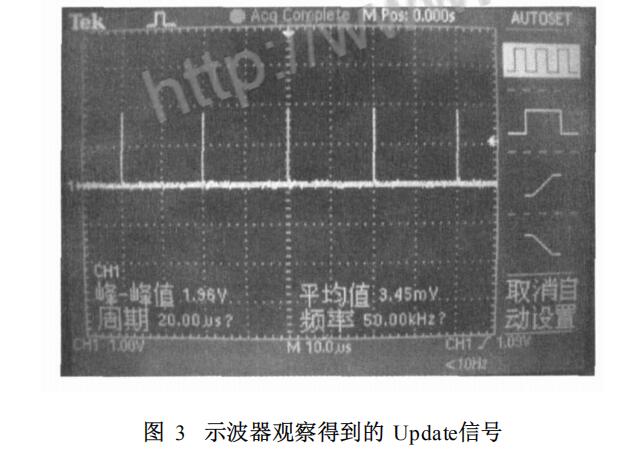
From the observed waveforms, it can be seen that the period of the update signal is 20 μs and the frequency of the output waveform is 789.2 9kHz, which is consistent with the initial set value. It can be seen that the experimental procedure is correct.
There is a rule, custom laptop is called programming laptop cause nearly 90% is used for projects. 15.6 inch laptop for coding and programming is usually equipped with 10th or 11th cpu, 2gb or 4gb graphics optional. 15 inch laptop untuk programming is used on big tender or group for a special jobs. 15.6 inch programming laptop under 30000 is a more competitive one for business or high school students or teachers.
However, here is the recommended laptop for programming, especially for heavy office jobs or university coursework, since double heat-releasing, metal body, bigger battery, FHD screen, high-level cpu, etc. Build the deep and stable foundation to enjoy smooth running experience. Your clients will satisfy it`s excellent performance. Of course, there are other lower specification with tight budget.
As a entry windows laptop for programming, this 14 inch celeron Education Laptop is the most competitive and hottest device for elementary project.
Any other special requirements, just contact us freely.
Programming Laptop,Laptop For Coding And Programming,Programming Laptop Under 30000,Recommended Laptop For Programming,Windows Laptop For Programming
Henan Shuyi Electronics Co., Ltd. , https://www.shuyiaiopc.com