
Wearable technology is sought after by users because they help to analyze people's daily activities and exchange information in an intuitive way, greatly improving our lifestyle and bringing us convenience. There are a variety of wearable electronic devices on the market, most notably smart watches, activity monitors and fitness bracelets. These highly portable devices are worn on the user or otherwise attached to the person and can measure and capture information through one or more sensors (see Figure 1).
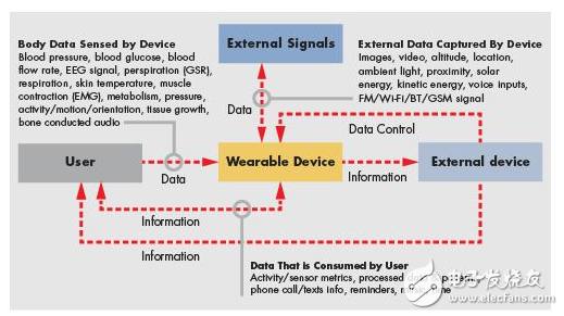
Figure 1: A typical wearable device integrates user data and external data. It works with an external device to analyze and display information to the user.
These devices continuously monitor user activity, even when they are sleeping. They run a variety of complex algorithms to extract meaningful information. For example: the wearer's sleep situation, and display the monitoring results to the user through an intuitive way and wireless interface. Because these devices provide important information that can change user activity, they must be reliable and accurate. In addition, in order to maximize battery life, they should be as efficient as possible.
Wearable devices typically have one or more sensors, storage devices, connectivity devices (RF controllers), a display, and a battery (see Figure 2). In addition to high functionality, reliability, and energy efficiency, wearables should be small, lightweight, and inexpensive, and can support a variety of different communication modes.
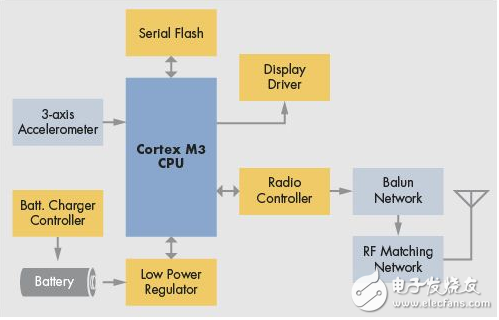
Figure 2: Block diagram of a wearable device showing the MCU, sensors, flash memory, battery and power management devices, connectivity subsystem, and display.
Existing communication protocols on the market include standard protocols such as ZigBee, Wi-Fi, Classic Bluetooth, and various proprietary protocols developed by chip vendors. Standard protocols are not designed to consider low power consumption as an important feature, so for a long time, most OE vendors chose to use proprietary protocols in their low-power products. However, using these proprietary protocols creates a lot of interoperability limitations and reduces design flexibility.
To eliminate these limitations and create an interoperable environment, the Bluetooth Technology Alliance (SIG) has introduced a new Bluetooth version, Bluetooth Smart, a wireless standard designed to achieve short-range communication with minimal power consumption.
Advantages of Bluetooth Smart
Like the classic Bluetooth protocol, the Bluetooth Smart Protocol works in the 2.4 GHz ISM band with a bandwidth of 1 Mbps. But unlike the classic Bluetooth protocol, the Bluetooth Smart Protocol offers a number of features for low-power wearable applications. Its low data rate makes it ideal for applications that only need to exchange status information. The protocol is optimized to deliver a small amount of bursts at regular intervals, allowing the host to maintain ultra-low power modes while transmitting information. In addition, it reduces the time it takes to establish a data exchange connection to a few milliseconds.
Each layer of the Bluetooth Smart Architecture is optimized to reduce power consumption. For example, it uses a larger physical layer modulation index than the classic Bluetooth protocol, which helps to reduce the transmit and receive current. The link layer is also optimized for fast reconnection, which reduces power consumption. The controller is responsible for performing various important tasks, such as establishing connections and ignoring duplicate packets, thus allowing the host to maintain a low power mode for a longer period of time.
The Bluetooth Smart Protocol has a reliable architecture similar to the classic Bluetooth protocol and supports adaptive frequency hopping and 32-bit CRC. In addition, it supports a special mode called "broadcast mode" that allows devices to transfer information without having to perform a linker.
The Bluetooth Smart Protocol is ideal for wearable devices for the following reasons:
- The protocol is optimized for ultra low power consumption;
- Low-power design helps reduce battery size, thereby reducing cost, size and weight of the product;
- Support for wearable devices that exchange small amounts of burst information over long intervals;
- Easy to promote, because the Bluetooth enabled host (a dual-mode device that supports classic Bluetooth and Bluetooth Smart Protocol) is built into the smartphone. This is in stark contrast to proprietary protocols that require additional effort by vendors to ensure connectivity.
A typical usage pattern for wearable devices offers multiple opportunities for devices to enter ultra low power or standby mode (see Figure 3).
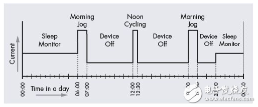
Figure 3: The normal use mode of wearable devices such as activity monitors offers several opportunities for devices to enter ultra low power or even standby mode.
Even during the event, the wearable device does not have to continuously send data. Whether it is the motion data measured by the three-axis accelerometer or the heart rate sensed by the sensor, the data is transmitted periodically, usually every connection interval. The normal procedure is to sense the data, convert the data, and then send the data over a Bluetooth smart connection. The rest of the time, the system is in deep sleep mode. Note that most existing chip solutions offer multiple power modes that can be traded between current consumption and wake-up time in a given power mode. Different modes should be selected according to the time requirements of the system.
It must be noted that the communication protocol is only one aspect of the wearable design. In addition to the communication interface, the wearable device also includes a sensor, an analog front end (AFE) for processing sensor signals, a digital signal processor for filtering environmental noise, a storage device for storing information, and one for implementation. A variety of other system-related functions of the processor, a battery charger and other modules. When designing a system, we need all of these components to achieve the lowest power consumption.
Optical heart rate monitoring
Let's take a wristband that monitors heart rate (see Figure 4). The optical heart rate monitor works on a photoplethysmographic pulse wave (PPG) technique that generates heart rate data by processing changes in blood volume. The technology uses an LED to illuminate human tissue and uses a photodiode to measure reflected signals, which contain information on changes in blood volume. A transimpedance amplifier (TIA) converts the photocurrent into a voltage that is then converted to a digital signal by an analog-to-digital converter (ADC). This digital signal is then processed in the firmware of the wristband processor to remove DC offset and high frequency noise to detect heart rate; in addition, active filters can be used to filter in the analog domain.
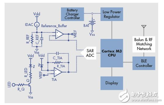
Figure 4: The wristband heart rate monitor analyzes changes in the optical signal caused by changes in blood volume at the sensor. A photodiode reads the reflected signal and a transimpedance amplifier converts the photocurrent into a voltage. The analog signal must be converted to a digital signal and then filtered to obtain heart rate data.
After the data analysis is completed, the device uses a Bluetooth link to send heart rate data to the Bluetooth smart controller on the wristband or device that supports the Bluetooth Smart Protocol. In some optical heart rate monitors, the wearable device processes heart rate data using a separate controller that communicates with the host processor via the I2C/SPI/IART protocol.
In these systems, the use of multiple discrete components not only adds to the complexity of the system in terms of electrical compatibility and testing, but also increases power consumption (because of the lack of control over AFE when not in use), BOM cost and PCB size .
To address these issues, multiple vendors have introduced devices based on a system-on-a-chip (SoC) architecture. These devices not only have a built-in controller, but also include analog and digital systems that can be used to implement most basic AFE and digital functions. One of the controllers is PSoC 4 BLE based on the Cypress Programmable System-on-Chip (PSoC) architecture. Designed for the wearable market, the SoC includes an 8-MHz ARM Cortex M0 CPU, numerous configurable analog and digital resources, and a built-in Bluetooth Smart Subsystem (see Figure 5).
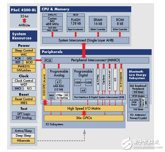
Figure 5: PSoC 4 BLE includes a processor, memory device, connectivity device, power management device, and analog and digital resources in one package.
In the analog front end, the device is equipped with four unconfigured op amps, two low-power comparators, a high-speed SAR ADC, and a dedicated capacitive sensing module for user interface applications. In terms of digital, it is equipped with two serial communication modules (SCB) for implementing I2C/UART/SPI protocol, four 16-bit hardware timer counter PWM (TCPWM) and four for digital logic implementation in hardware. Universal Digital Module (UDB) (like an FPGA).
To demonstrate the benefits of the SoC architecture, let's take a look at what happens to the heart rate monitor shown in Figure 4 after using PSoC 4 BLE (see Figure 6). In this release, the SoC implements all its features using its internal resources. Beyond this controller, only a few passive components and one transistor for driving the LEDs belonging to the RF matching network are required. This integrated architecture eliminates BOM cost and PCB size while allowing designers to control the power consumption of the AFE.
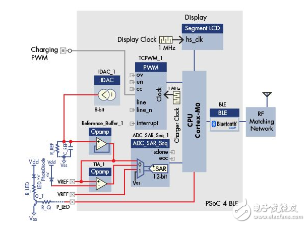
Figure 6: The SoC architecture of the wristband heart rate detector reduces the size, BOM cost and complexity of the design.
In addition to these advantages, using the SoC architecture also helps to reduce time-to-market for the following reasons:
- A ready-to-use firmware IP provides support for system development.
- Since each module belongs to the same chip, they can cooperate with each other without delay. Developers don't have to worry about how to dock them, check their logic levels, or resolve interoperability issues. All of these issues have been resolved within the device.
- A configurable environment that flexibly integrates last minute design changes.
In some designs, a Cortex-M0 core may not be sufficient to meet processing power requirements. In this case, a Cortex-M3 core (such as PSoC 5LP) can be used to handle system-related functions, using a Bluetooth Smart SoC (such as PSoC 4 BLE) to control Bluetooth communication as well as AFE and digital logic.
The increasing popularity of devices such as smartphones that support Bluetooth smart protocols and the low power consumption of Bluetooth smart technology make Bluetooth smart the de facto standard for wearable products. Bluetooth Smart enables low-power design at all protocol layers and, as a standard protocol, it also supports interoperability. By leveraging SoCs for the wearables market, embedded engineers can reduce the size, power, BOM cost, complexity and time-to-market of their devices to bring better products to market faster.
Jilin Nengxing Electrical Equipment Co. Ltd. , https://www.nengxingelectric.com