
Wave Port is a typical external port in HFSS. The term “outside†refers to the field distribution on only one side, which is generally at the boundary between the boundary and the background. The external port needs to pass the transmission line to add the excitation signal to the structure, and the external port is usually defined as the cross section of the transmission line. The Wave Port section is the reference plane for HFSS to solve structural parameters. It is very important for the phase calculation of S parameters. The HFSS solves the characteristics of the transmission line at the port section, and obtains the characteristic impedance and propagation constant of the port for calculating the S parameter.
1. Transmission line prototype:The transmission line width is W=6mil, the line spacing is S=3W=18mil, the line length is 2000mil, the laminated structure is 1.4mil copper thickness, the transmission line is 58mil away from the GND plane below, and the dielectric constant of the medium is 4.25, as shown below:
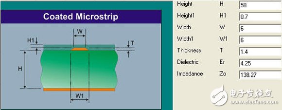
The characteristic impedance of the transmission line calculated by Polar from the above figure is 138.27 ohm.
2. The airbox background acts as a Wave Port:Create the Wave Port on the Boundary face of free space and let the Wave Port plane fit the transmission line, as shown below:
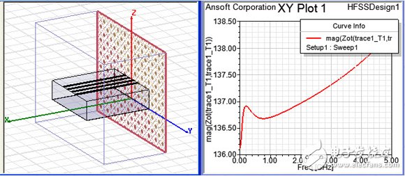
As can be seen from the above figure, the impedance of the transmission line calculated by HFSS is approximately 136.7~138.5 ohms. This result is in complete agreement with the calculated characteristic impedance of Polar in the prototype.
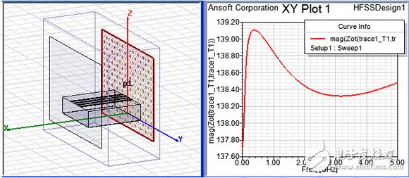
3. Use the YZ plane on the side of the PCB as the Wave Port:Create the Wave Port on the side YZ plane of the PCB and let the Wave Port plane close to the free space, as shown below:
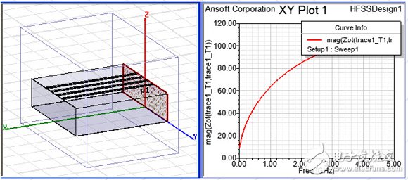
As can be seen from the above figure, the simulated characteristic impedance has a large change with frequency. This is because the Wave Port does not consider the electromagnetic field effect of the space above the transmission line, so the result is wrong.
4.Wave Port port does not cling to free space:Create the Wave Port on the YZ plane on the side of the PCB, but leave the Wave Port plane not close to the free space, as shown below:
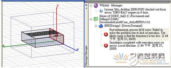
As can be seen from the above figure, HFSS cannot continue the simulation because it does not consider the electromagnetic field effect of the space above the transmission line, and there is no electromagnetic field informaTIon in the space between the free space boundary and the Wave Port on the side of the PCB.
5. The new Wave Port port plane does not cling to free space:On the YZ plane of the side of the PCB, another "rectangular plane" is built. The plane is close to the transmission line but does not stick to the free sapce boundary. Set the Wave Port on this new plane, as shown below:
The above figure shows that the characteristic impedance of the transmission line obtained by HFSS simulation is about 223.9 ohm, which is very different from the calculation result of Polar. This result is wrong.
6. Add the big port of the Wave Port port and stick to the free space:On the YZ plane of the side of the PCB, another "rectangular plane" is built. The plane is close to the transmission line and close to the free sapce boundary. The lower part of the plane is beyond the lower edge of the PCB. Set the Wave Port on this new plane, as shown below:
As shown in the above figure, the impedance of the transmission line calculated by HFSS is about 136.7~138.5 ohms. This result is in complete agreement with the calculated characteristic impedance of Polar in the prototype.
Bacteria are everywhere in our daily lives. Mobile phones have become an indispensable item for us. Of course, bacteria will inevitably grow on the phone screen. The antimicrobial coating used in our Anti Microbial Screen Protector can reduce 99% of the bacterial growth on the screen, giving you more peace of mind.
Self-healing function
The Screen Protector can automatically repair tiny scratches and bubbles within 24 hours.
Clear and vivid
A transparent protective layer that provides the same visual experience as the device itself.
Sensitive touch
The 0.14mm Ultra-Thin Protective Film can maintain the sensitivity of the touch screen to accurately respond to your touch. Like swiping on the device screen.
Oleophobic and waterproof
Anti-fingerprint and oil-proof design can help keep the screen clean and clear.
If you want to know more about Anti Microbial Screen Protector products, please click Product Details to view the parameters, models, pictures, prices and other information about Anti Microbial Screen Protector products.
Whether you are a group or an individual, we will try our best to provide you with accurate and comprehensive information about Anti Microbial Screen Protector!
Antimicrobial Screen Protector, Anti-microbial Screen Protector, Anti-bacterial Screen Protector, Antibacterial Screen Protector,Anti-microbial Hydrogel Screen Protector
Shenzhen Jianjiantong Technology Co., Ltd. , https://www.jjthydrogelprotector.com