
Compared to low-frequency circuits, complicated circuit matching is required, and the structure of high-frequency circuits is relatively simple. A simple structure often means that more problems need to be considered. Take the most common AC coupling capacitors, either adding two direct connections between the chips or two between the chip and the connector. Seemingly simple, but everything is different because of the high speed. The high speed makes this capacitor not "ideal". This capacitor is not designed well and may cause the entire project to fail. Therefore, for high-speed circuits, this AC coupling capacitor will not be optimized and will be "fatal."
Following the author's previous experience in the project, the inventory analysis of some of the problems I encountered in the use of this capacitor.
Begin to understand the role of AC coupling capacitors first. In general, we use AC coupling capacitors to provide DC bias, which is to filter out the DC component of the signal and make the signal symmetrical about the 0 axis. Since this is the role, can this capacitor be placed anywhere on the channel? This is the first question that I encountered when using this capacitor when I was first working on a high-frequency circuit—where the AC coupling capacitor should be placed.
Here we take a typical project to analyze the path.
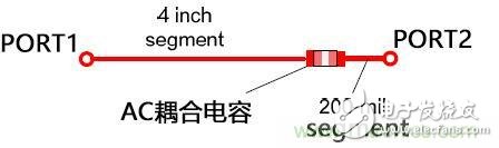
Figure 1: AC Coupling Capacitor Typical Path
In low-speed circuit design, this capacitor can be equivalent to an ideal capacitor. In high-frequency circuits, due to the presence of parasitic inductances and the impedance discontinuities caused by the plates, in fact, this capacitor cannot be considered as an ideal capacitor. The signal frequency here is 2.5G, the channel length is 4000mil, and the position of the AC coupling capacitor is located at the distance of 200mil from the sending end and the receiving end, respectively. Let's take a look at the changes in the simulated eye diagram.
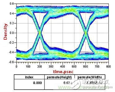
Figure 2: Eye diagram of AC coupling capacitor close to the transmitter
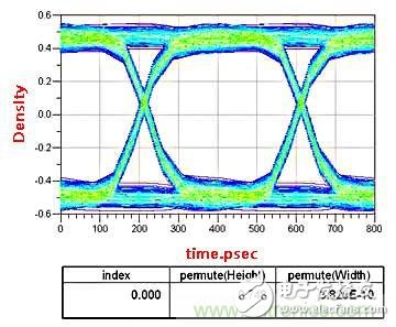
Figure 3: Eye Diagram of AC Coupling Capacitor Close to Receiver
Obviously, the integrity of the signal when the AC coupling capacitor is close to the receiving end is better than that at the transmitting end. My understanding is this: non-ideal capacitor impedance is not continuous, the signal reflected by the channel after the reflected energy is less than the direct reflection of energy, so the vast majority of serial links require this AC coupling capacitor on the receiving end. However, there are some exceptions. I previously encountered this problem when I was doing board-to-board connection. I checked the PCIE specification and found that if two boards are usually placed on the transmitting end, another function of the AC coupling capacitor is also used - overvoltage protection. For example SATA, so it is usually required to place near the connector.
Solved the problem of placement, another problem that plagued everyone is the choice of the value of the value. In this case, the equivalent resistance R of our entire serial link is fixed, then the selection of the AC coupling capacitor C will be related to the time constant (RC). The larger the RC, the greater the DC component, the higher the DC voltage. The lower the drop. In this case, AC coupling capacitance can increase infinitely? Obviously it is not enough.
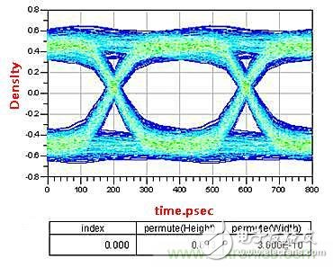
Figure 4: Measured eye diagram with increased AC coupling capacitance
In the same position, compared with FIG. 3, it can be seen that the eye height becomes lower after increasing the coupling capacitance. The reason is that "high speed" makes the capacitance unsatisfactory. The induced inductance will generate series resonance. The larger the capacitance, the lower the resonance frequency. The AC coupling capacitance is inductive at low frequencies, so the attenuation of high frequency components increases, the eye height decreases, the rising edge slows, and the corresponding JITTER will also Increase. It is usually recommended that the AC coupling capacitance is between 0.01uf and 0.2uf, and 0.1uf is more common in the project. The 0402 package is recommended.
Finally, solve the above two problems, and then analyze the optimal design of this capacitor from the PCB design. Actually in the project, compared to the visible factors such as the location and capacitance of the AC coupling capacitor, the more elusive is the plate itself (including the accuracy of the pad, the uniformity of the copper foil, etc.) and the parasitic capacitance at the pad. The effect of signal integrity. We know that high-frequency signals must travel along a path with uniform characteristic impedances. If impedance mismatch or discontinuity is encountered, some signals will be reflected back to the transmitting end, causing signal attenuation and affecting signal integrity. In the project, this situation usually occurs at the pad or board connector. This problem was often encountered when the author first addressed the high-speed circuit design.
To solve this problem, we must start from two aspects. First of all, in the selection of the plate, we usually use high-performance ROGERS plate in the application. Rogers plate is very precise in the control of the thickness of the copper foil, uniform copper foil coverage greatly reduces the impedance discontinuity; then in the elimination of welding A common solution in the parasitic capacitance of the disc is to perform interlayer processing at the pad (hollowing out the reference plane area directly below the pad, and creating a copper padding on the inner layer) by increasing the pad and its reference plane ( Or is the distance between the return paths, reducing the discontinuity of the capacitance. In the author's project, the use of ROGERS plates with uniform medium and precisely controlled copper foil width also effectively improves the processing accuracy of the pad.
Compare the signal integrity of the ROGERS plate before and after precise spacer treatment by simulation.
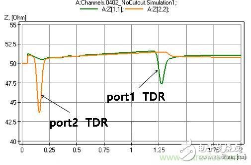
Figure 5: TDR before spacer treatment
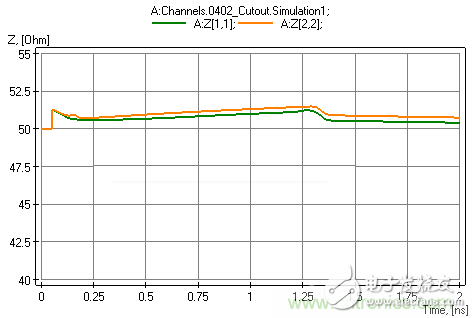
Figure 6: TDR after spacer processing
Comparing Fig. 5 with Fig. 6, it is found that the impedance jump before treatment is obvious, and the impedance after the interlayer treatment is improved much, with almost no steps and discontinuities.
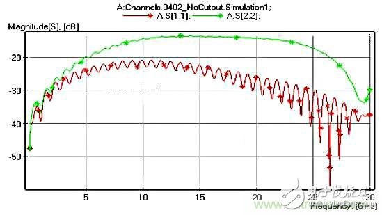
Figure 7: Return Loss before Interlayer Treatment
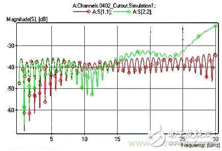
Figure 8: Return Loss after Interlayer Treatment
Comparison of Figure 7 with Figure 8 shows that after using ROGERS plate as a spacer, the return loss is reduced to -30 dB compared to the untreated layer, which greatly reduces the return loss and ensures the integrity of the signal transmission.
In summary, if you want to get the “fatal†AC coupling capacitor in high-frequency circuits, not only do you have to do homework on the design of the circuit, but at the same time, choosing a high-frequency PCB board material with better performance will allow you to do more with less.
Arts And Crafts Zinc Casting,Cold Chamber Die Casting,Aluminium Gravity Die Casting,Gravity Die Casting Parts
Dongguan Metalwork Technology Co., LTD. , https://www.dgdiecastpro.com