
Abstract: A video compression and decompression card based on wavelet video codec chip is proposed, and its hardware implementation is described in detail.
This article refers to the address: http://
Keywords: wavelet transform ADV612 dedicated chip IIC bus video capture and compression
As a signal analysis method, wavelet transform has the advantages of multi-scale, multi-resolution analysis and time domain localization and frequency domain localization. Wavelet transform is a transform that is freely scalable on frequency. When the signal bandwidth is narrow, it can make the marking of the narrowband signal finer by narrowing down; when the signal bandwidth is wide, it can make the description meet the precision requirement by means of amplification. Therefore, wavelet transform is an image compression method that is not constrained by bandwidth. Compared with the traditional DCT transform-based coding method, the image coding based on wavelet transform transforms the whole image, which makes full use of the overall correlation of the image and eliminates the block effect brought by the traditional block coding method. The wavelet series can approximate a function at different resolutions to achieve multi-resolution decomposition. Multi-resolution decomposition allows us to approximate the source image with different characterization accuracy, compressing the original image at different levels, breaking the compression ratio limitation of the traditional encoding method, and obtaining a high compression ratio. The superior performance of wavelet transform has been widely used in the field of video image coding. At present, a dedicated chip for image coding using wavelet transform has been introduced.
 This paper introduces the wavelet video codec dedicated chip ADV612, and describes the design and implementation of the video compression card based on ADV612.
1 Wavelet video codec dedicated chip ADV612
1.1 ADV612 system function introduction
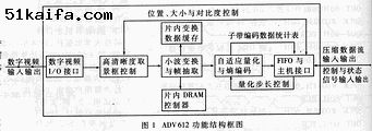
ADV612 is the core component of the video card described in this article. It is a dedicated chip for video encoding and decoding of wavelet video released by ANALOG. The ADV612 uses high-density GMOS integrated circuit technology. The entire chip consists of digital video I/O interface, high-definition viewfinder control, wavelet transform and frame extraction, on-chip SRAM, on-chip DRAM controller, adaptive quantizer and entropy encoder. The FIFO compressed data cache is combined with functional modules such as the host interface, as shown in Figure 1.
The digital video I/O interface supports the CCIR601 international standard format. When encoding, the digital video is input from the digital video interface, and is subjected to frame extraction and wavelet transform, and sent to the quantizer for quantization. The quantized data is sent to an entropy encoder for run-length encoding and Huffman encoding to produce a final compressed data stream that is fed into a 512 x 32-bit FIFO buffer integrated into the chip. When the amount of data in the on-chip FIFO reaches the preset value of the host, the ADV612 issues an interrupt to notify the host to take the data. In contrast to the decoding process, the compressed data is sent to the FIFO by the host, and the decoded data and video data of the CCIR601 format are generated and output from the digital video interface.
1.2 Characteristics of ADV612
1.2.1 High Definition Frame Function
The ADV612 supports a feature called high definition viewfinder. This feature allows a rectangular area in a frame to have a lower compression ratio relative to other areas (which we call the background), or no compression at all. The position and size of the rectangular area and the contrast to the background are controlled by the host via the host interface input control word of the ADV612. This function provides a shortcut for the user to select a region of interest for high-definition display without affecting the compression ratio, thereby making the whole system particularly suitable for monitoring applications.
 1.2.2 Accurate code stream control
The ADV612's adaptive quantizer allows the host to control the quantization step size. The host calculates the quantization step size of the next frame by counting the data of the previous frame image subband encoded data, and writes it to the quantization step size register before the next frame compression starts. Through the quantization step control, the host can obtain a stable compressed stream output. This is particularly advantageous for network transmissions with limited bandwidth, such that they do not cause sudden changes in the compressed code stream due to drastic changes in image content, causing network congestion.
1.2.3 Hardware coding to achieve wavelet transform
Considering the huge computational complexity of the wavelet transform, the wavelet transform module of ADV612 uses the hardware coding method to realize the wavelet transform and wavelet inverse transform with Morlet wavelet as the orthogonal wavelet base, which ensures that the video signal can be processed in real time. An on-chip SRAM is integrated on-chip for use as a high-speed data buffer for conversion.
1.3 Host Interface of ADV612
The ADV612 integrates several control word registers and status registers on-chip for the parameters required to store the host's ADV612 codec and reflect the operating status. The control word registers and status registers are called indirect registers, and the ADV612 addresses the control word registers and status registers in a unified manner. The host cannot directly access the indirect registers.
To access the indirect registers and the on-chip FIFO, the ADV612 sets up a set of registers that are directly accessible by the host, called direct registers. There are four 32-bit direct registers: an indirect address register, an indirect data register, a compressed data register, an interrupt control, and a status register. The indirect address register stores the address of the indirect register to be accessed; the indirect data register stores the data read from the indirect register or to be written to the interleave register; the compressed data register is the mapping of the on-chip FIFO, and reading and writing the register will place the data. Read or write to the FIFO; the upper 16 bits of the interrupt control and status registers are control bits that set the condition that causes the ADV612 to issue an interrupt to the host. The lower 16 bits are status bits that reflect the cause of the current interrupt.
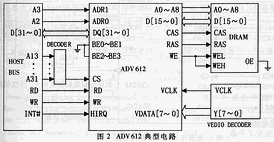
 The host interface of the ADV612 includes: 32-bit data bus (D31 to D0), two-bit address line (ADR1ADR0), chip select signal (CS), read signal (RD), write signal (WR), response signal (ACK), and interrupt. Output (INT). Two address lines are used to select four direct registers:
ADR1, ADR0=(0,0) Indirect Address Register
(0,1) indirect data register
(1,0) compressed data register
(1,1) interrupt control and status register
The ADV612 uses the response signal (ACK) to inform the host whether the operation is successful or not. If the response signal is low, the operation is successful and the next operation can be performed.
1.4 Typical Circuit of ADV612
A typical circuit for the ADV612 is shown in Figure 2.
2 video card design and implementation
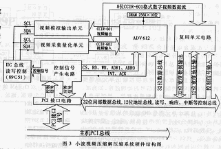
The video card is composed of multiple unit modules such as analog video acquisition and quantization, video compression and decompression, control signal generation, 8-bit to 32-bit multiplexing, video analog output, and PCI bus interface, as shown in FIG.
2.1 Video Acquisition Quantization Unit
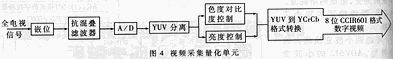 The full TV signal input from the video input jack first passes through the unit. The unit first clamps and anti-aliasing the analog signal. The filtered signal is sent to the A/D conversion circuit for analog-to-digital conversion, and the digital video enters the Y/C separation circuit for Y/C separation. The separated Y and UV signals are respectively sent to the brightness control and chromaticity contrast control circuits. In the brightness control circuit and the chrominance control circuit, the signal levels of luminance and chrominance are enhanced or attenuated according to user preset values. The Y, U, V signals processed by the luminance chrominance are converted into the international standard CCIR 601 video data stream input to the video compression decompression unit in the YUV to YcrCb conversion circuit. The video acquisition quantization unit block diagram is shown in Figure 4.
2.2 Video Analog Output Unit
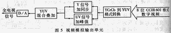
The video signal entering the unit passes through the YcrCb to YUV conversion circuit, and is converted into Y and UV signals by the YcrCb signal. The Y signal enters the synchronization circuit to superimpose the video synchronization signal, and the UV signal enters the peak circuit to add the peak signal. The Y signal added to the video sync and the UV signal added to the peak are mixed in the hybrid circuit, and the YUV digital video is converted into an analog full TV signal through the D/A conversion circuit, and is output from the analog port. The video analog output unit is shown in Figure 5.
 Both the video acquisition quantization unit and the video analog output unit require the host to set the control word to control the processing of the video signal, such as brightness, chrominance level control, band selection of band pass filtering, and the like. The control interface of the video acquisition and quantization unit and the video analog output unit adopts an IIC bus interface, and both units are slave devices of the IIC bus. The IIC bus is a serial bus developed by Philips. Through a clock line and a data line, the IIC master on the bus can communicate with the IIC slave. The video card uses the two serial ports of the 89C51 single-chip microcomputer to simulate the clock line and data line of the IIC bus. The control signal of the single-chip microcomputer is generated by the control generating circuit.
2.3 video compression decompression unit
The video compression decompression unit is composed of ADV612 and a 256K×16Bit DRAM to complete the encoding and decoding of digital video. The host interface of the ADV612 is directly attached to the user bus of the PCI interface unit. The on-chip FIFO of the ADV612 maps a 512 x 32-bit contiguous memory in the host memory address space through the PCI interface circuit. The direct register of the ADV612 maps four consecutive I/O addresses in the host I/O space. The RD, WR, CS, ADR1, and ADR0 required by the ADV612 are generated by the control generation circuit. The control generation circuit is completed by a piece of EPLD. 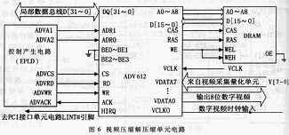 It translates the read/write, chip select, and interrupt signals of the PCI interface unit circuit, and decodes the address signals to generate the chip select and read/write signals required by the ADV612 and the read, write, and interrupt required by the IIC read/write controller 89C51. The control signal, at the same time it sends the response signals of the 89C51 and ADV612 to the PCI interface unit circuit. The video compression and decompression unit circuit is shown in Figure 6.
2.4 Multiplex unit circuit
The multiplexing unit circuit is composed of 8-bit to 32-bit data multiplexing and multiplexed data buffer, as shown in FIG.
The multiplex unit circuit only starts to work when the video card is in the decompressed state. The multiplexing circuit consists of an EPLD that multiplexes 8-bit video data into 32-bit wide data driven by a video clock. The purpose of multiplexing is to take full advantage of the 32-bit data bus of the PCI bus. The multiplexed data is written into the dual port RAM as a data buffer. One port of the dual port RAM is controlled by a multiplexing circuit that generates data, address, chip select and write signals; the address signal and read signal of the other port are from the PCI interface circuit. When the amount of data in the dual-port RAM reaches the preset value, the EPLD issues an interrupt to notify the host to take the data in the dual-port RAM.
2.5 PCI interface unit circuit
The PCI interface unit circuit performs the function of the PCI bus to the bridge of the local logic circuit on the board. 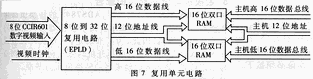 On the one hand, it implements various protocols and specifications for interfacing with the PCI bus; on the other hand, it translates PCI bus signals into operations on local logic circuits, and generates various controls for local logic such as interrupt, chip select, read and write, etc. The response signal of the local logic is also translated into the response of the PCI bus, and the interrupt signal is converted into an interrupt to the PCI bus, and the host local logic circuit is notified that the host needs to participate in the operation.
3 compression card performance
The video card can work in both encoding and decoding states: when encoding, it can capture the full TV signal input by the camera from the analog video input port, quantize and compress the analog video signal; and decompress the compressed data sent by the host in real time during decoding. The stream, output digital video signal can be converted to full TV signal output to the analog video interface by D/A. The compression card has the following features: the user can control the position and compression degree of the high-definition area; the precise code stream control, the output compression code rate is stable; the high-speed data transmission, the peak rate of interaction with the host can reach 132MB/s. The wide range of performance parameters of the wavelet compression decompression card allows the system to operate under a variety of different network bandwidths. Table 1 shows the video card performance parameter table.
Table 1 Video card performance parameter table
| parameter | Minimum value | Maximum |
| Compression ratio | 4:1 | 7500:1 |
| Output frame rate | 0.5 frames/second | 30 frames / sec |
| Compressed data output rate | 28.8kB/s |
All In One Business Computer is the one of the important All In One PC series, can meet all enter and normal business application scenarios. Therefore, more and more clients choose and recommend this Business All In One Computer for business or education projects. The Best All In One Computer For Business is the similar Apple design, competitive and attractive, the hottest parameters is 19 or 21.5 inch intel i3 or i5 2th or 3th or 4th 4 gb ram 128GB ssd . There are many other all In One Computers For Business with lighter weight. Of course, you can see Colorful All In One Gaming PC, All In One Desktop Touch Screen and All In One Business Pc. Believe you can always find the right one at this store. To save time, You can also contact us by email or calling directly to get matched and valuable information fast.
Any other special configuration interest, also feel free to let us know, will try our best to back you up.
Except all in one Custom All In One PC, 14 inch Education Laptop and 15.6 inch business laptop also available here.
All In One Business Computer,Business All In One Computer,Best All In One Computer For Business,all In One Computers For Business,All In One Business Pc
Henan Shuyi Electronics Co., Ltd. , https://www.shuyielectronics.com