
In electronic technology, the N/2 (N is an odd-numbered) frequency-dividing circuit has an important application. For a specific input frequency, the required output can be obtained by dividing by N/2, which requires the circuit to have N/. A non-integer multiple of the frequency division function of 2. The CD4013 is a dual-D flip-flop. It is convenient to form an N/2 frequency dividing circuit based on a number of two-way circuits composed mainly of CD4013 and feedback control such as XOR gate.
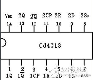
The CD4013 consists of two identical, independent data-type flip-flops. Each flip-flop has independent data, set, reset, clock input, and Q and Q outputs. This device can be used as a shift register and can be used as a counter and flip-flop by connecting the Q output to a data input. When triggered by the rising edge of the clock, the logic level applied to the D input is transferred to the Q output. Set and reset are independent of the clock and are completed by a high on the set or reset line, respectively.
The initial state of the circuit is in the reset state, and the terminals Q1 and Q2 are both low. When the fi signal is input, the output is also controlled by the feedback of the Q2 terminal of the flip-flop IC2 due to the action of the XOR gate on the input terminal (the attached table is the XOR gate logic function table) (the non-gate F2 is an increased first-order delay gate, The A point waveform is the same as Q2). Under the action of the rising edge of the first fi clock pulse, the flip-flops IC1 and IC2 are flipped. Due to the feedback effect of the Q2 terminal, the XOR gate outputs a very narrow positive pulse, and the width is determined by the delay of the two-stage D flip-flop and the inverting gate. When the first fi pulse jumps, the XOR gate output jumps up again, causing the IC1 flip-flop to flip again, and the IC2 flip-flop state is unchanged. Thus, during the half cycle of the first input clock, the clock terminal CL1 of the IC1 flip-flop has a full-cycle input, but under the influence of a subsequent input clock, the Q2 terminal of the IC2 flip-flop is at a high level. The clock input of the IC1 flip-flop follows the fi signal (inverted or in phase). Originally, the IC1 flip-flop inputs two complete input pulses to output a full-cycle pulse. Now, due to the feedback control of the XOR gate and the Q2 terminal of the IC2 flip-flop, a pulse output of one cycle is obtained under the action of the first fi pulse. Therefore, one half clock pulse per input is achieved, and a full cycle output is obtained at the Q1 end of the IC1 flip-flop.
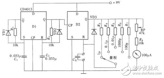
CD4013 frequency division circuit diagram
3.2v12-30Ah Lithium Battery Cells
3.2v12-30Ah Lithium Battery Cells,3.2v12-30Ah Lithium Battery Cells price,3.2v12-30Ah Lithium Battery Cells product
Jiangsu Zhitai New Energy Technology Co.,Ltd , https://www.zhitainewenergy.com