
First, the working principle of FET - - concept
A field effect transistor (FET) is an abbreviation for a field-effect transistor. Since it is only conductive by majority carriers in a semiconductor, also known as a unipolar FET , it is a common use of input circuits. A voltage-controlled semiconductor device that controls the output loop current by the electric field effect. The FET has the advantages of small size, light weight, long life, and the internal resistance of the input circuit is as high as 107~1012Ω, and the noise is low. It has good thermal stability, strong radiation resistance, and lower power consumption than the latter. These advantages have been widely used in various electronic circuits since its birth in the 1960s.

Second, the working principle of the field effect tube - - structure
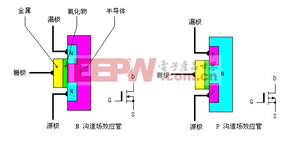
All FETs have three gates: gate g (gate), drain d (drain), and source s (source), which correspond to the base b (base), collector c (collector) of the bipolar transistor, and Emitter e (emitter). In addition to the junction field effect transistor, all FETs also have a fourth end, referred to as a body, a base, a bulk, or a substrate. A depletion layer is formed at the interface between the P region and the N region, and a non-depletion layer region between the drain d and the source s is referred to as a conductive channel.
Third, the working principle of FET - - classification
The FET can be divided into a junction field effect transistor ( JFET ) and an insulated gate field effect transistor (JGFET). The junction field effect transistor ( JFET ) is named after two PN junctions, and the insulated gate field effect transistor ( JGFET) is named after the gate is completely insulated from other electrodes. Since the gate of the insulated gate field effect transistor is metal aluminum, it is also called a MOS transistor.
The FET is divided according to the difference of the conductive mode, and can be divided into a depletion type and an enhancement type. When the gate voltage is zero, the larger drain current is called depletion type; when the gate voltage is zero, the drain current is also zero, and the drain current must be added after a certain gate voltage is added. .
Whether it is a junction FET or an insulated gate FET, whether it is a depletion FET or an enhanced FET, it can be divided into N-channel and P-channel, and its structure is shown in the figure below. :
Fourth, the FET working principle - - knot
The junction field effect transistor can be divided into an N-channel junction field effect transistor and a P-channel junction field effect transistor. Below we will describe the working principle of the junction field effect transistor by taking the N-channel as an example.
In order to ensure the normal operation of the N-channel junction field effect transistor, a negative voltage (ie, uGS<0) should be applied between the gate and the source to ensure that the depletion layer is subjected to the reverse voltage; The forward voltage uDS is used to form a drain current. The larger the negative voltage between the gate and the source, the thicker the depletion region formed at the interface of the PN junction, the narrower the conductive channel, the larger the channel resistance, and the smaller the drain current iD. Conversely, if the gate-source is The smaller the negative voltage is, the thinner the depletion region is, the wider the conduction channel is, the smaller the channel resistance is, and the larger the drain current iD is. Therefore, the control of the channel current between the gate-source negative voltage of the field effect transistor is realized.
For a P-channel junction field effect transistor, it is similar to the N-channel principle, but a forward voltage (ie, uGS>0) is applied between its gate and source to ensure that it can work normally.
Five, FET working principle - - Insulated grid
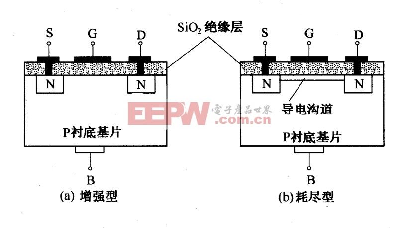
Taking an N-channel depletion MOS transistor as an example, if a large amount of positive ions are doped in the SiO2 insulating layer when manufacturing the MOS transistor, even if uGS=0, there is an inversion of the surface of the P-type substrate under the action of positive ions. There is a conductive channel between the layers, ie the drain-source. As long as a forward voltage is applied between the drain and the source, a drain current is generated, and when uGS is positive, the inversion layer becomes wider, the channel resistance becomes smaller, and the channel current iD increases; otherwise, when uGS is negative The inversion layer is narrowed, the channel resistance becomes large, and the iD is reduced. When uGS decreases from zero to a certain value, the inversion layer disappears and the conduction channel between the drain and source disappears, iD=0. The gate source voltage is controlled to the drain current.
Sixth, FET working principle - - Enhanced
Taking N-channel as an example, in an N-channel enhancement mode device, a forward voltage should be applied between the gate and source. The positive voltage attracts free moving electrons in the body to move toward the gate, forming a conductive channel. But first, sufficient electrons need to be attracted to the vicinity of the gate to counter the dopant ions added to the FET; this forms a region called the depletion region without moving carriers, a phenomenon known as Is the threshold voltage of the FET. A higher gate-to-source voltage will draw more electrons through the gate, creating a conductive channel from source to drain; this process is called "inversion."
Seven, FET working principle - - depletion type
In an N-channel depletion mode device, applying a negative voltage between the gate and source causes a depletion region to expand the width and invade the channel from the boundary, thereby narrowing the channel. If the depletion region is extended to completely close the channel, the channel resistance between the drain and source will become large, and the FET will be effectively turned off like a switch. Similarly, in a P-channel depletion mode device, applying a forward voltage between the gate and source will widen the channel and the channel resistance will be smaller, making the current easier to pass.
There are many kinds of FETs, but they are inseparable. The children's shoes of interest can also refer to the following article~~
1, FET working principle
2, mos FET working principle
3, field effect transistor amplifier
4, MOS tube working principle, it is so simple
5, the development trend of CMOS field effect transistors
Transistor
China leading manufacturers and suppliers of DC Support Capacitors,DC Capacitor, and we are specialize in Electrolytic capacitor,High Voltage Capacitor, etc.DCMJ DC Support Capacitors
DCMJ DC Support Capacitors,Capacitors High Voltage,Dc-link Filter Capacitor,Dc Film Capacitors
YANGZHOU POSITIONING TECH CO., LTD. , https://www.pst-thyristor.com