
1 Introduction
With the large number of applications of electronic devices, the role of power supplies in these devices is becoming more and more important, and switching converters account for a larger proportion in power supplies due to their small size, light weight, and high efficiency. Switching power supplies mostly operate at high frequencies. During the switching process of switching devices, high-frequency changes in energy in parasitic components (such as parasitic capacitance, parasitic inductance, etc.) generate a large amount of electromagnetic interference (EMI).
EMI signals occupy a wide frequency range and have a certain amplitude. The conduction and radiation in the circuit and space pollute the surrounding electromagnetic environment and affect the electromagnetic compatibility with other electronic devices. With the continuous improvement of electromagnetic interference and electromagnetic compatibility requirements of electronic equipment in recent years, research on electromagnetic interference and new suppression methods has become a hot spot in the research of switching power supplies.
This paper briefly introduces the mechanism of electromagnetic interference generation and propagation, and summarizes several new methods proposed in recent years to suppress the electromagnetic interference generation and propagation of switching power supplies.
The electromagnetic interference of switching power supplies has a great influence on the performance of electronic equipment. Therefore, various standards have become more and more demanding for suppressing electromagnetic interference of power supply equipment. The mechanism of electromagnetic interference generation in switching power supply is briefly described. Several new methods for suppressing electromagnetic interference proposed in recent years are summarized, and its principle and application are briefly introduced.
2 The way electromagnetic interference is generated and transmitted
The electromagnetic interference in the switching power supply is divided into two types: conducted interference and radiated interference. Generally, the conducted interference is better analyzed, and the circuit theory and mathematical knowledge can be combined to study the characteristics of various components in electromagnetic interference. However, for radiated interference, due to the comprehensive effects of different interference sources in the circuit, To the electromagnetic field theory, it is more difficult to analyze. A brief introduction to the mechanism of these two types of interference will be given below.
2.1 Generation and propagation of conducted interference
Conducted interference can be divided into Common Mode (CM) interference and Differential Mode (DM) interference. Due to the existence of parasitic parameters and the high frequency turn-on and turn-off of the switching device in the switching power supply, the switching power supply generates large common mode interference and differential mode interference at its input end (ie, the AC grid side).
2.1.1 Common Mode (CM) Interference
When the converter operates at high frequencies, the dv/dt is high, which excites the parasitic capacitance between the transformer coils and between the switch and the heat sink, resulting in common mode interference. As shown in Figure 1, the common mode interference current flows from the switch tube with high dv/dt through the grounded heat sink and ground, and then flows back to the input line by the high frequency LISN network (equivalent to two 50Ω resistors).
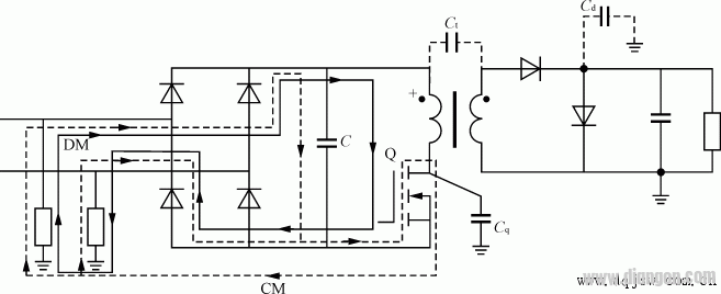
Fig.1 Propagation path of common mode and differential mode interference in a typical switching converter
According to the principle of common mode interference generation, the following several suppression methods are often used in practical applications:
1) Optimize circuit device layout to minimize parasitic and coupling capacitance.
2) Delay the opening and closing time of the switch. However, this is inconsistent with the trend of high frequency switching power supply.
3) Apply a buffer circuit to slow down the rate of change of dv/dt.
2.2.2 Differential Mode (DM) Interference
The current in the switching converter is switched at high frequency, resulting in a high di/dt on the input and output filter capacitors, ie, the interference voltage is induced at the equivalent inductance or impedance of the filter capacitor. Differential mode interference will occur at this time. Therefore, the use of high-quality filter capacitors (equivalent inductance or low impedance) can reduce differential mode interference.
2.2 Generation and spread of radiation interference
Radiated interference can be further divided into near-field interference [measurement point to field source distance <λ/6 (λ is the wavelength of the interference electromagnetic wave)] and far-field interference (measurement point and field source distance > λ/6). According to Maxwell's electromagnetic field theory, the changing current in the conductor will produce a changing magnetic field in its surrounding space, and the changing magnetic field will produce a changing electric field, both of which follow Maxwell's equation. The magnitude and frequency of this varying current determine the magnitude of the electromagnetic field generated and its range of action. In the radiation research, the antenna is the electromagnetic radiation source. In the switching power supply circuit, the components and wiring in the main circuit can be regarded as the antenna, which can be analyzed by the theory of electric dipole and magnetic dipole. In the analysis, diodes, switching tubes, capacitors, etc. can be regarded as electric dipoles; the inductive coil can be considered as a magnetic dipole, and then comprehensive analysis can be performed by the relevant electromagnetic field theory.
Figure 2 is a spatial distribution diagram of a Boost circuit. The components are regarded as electric dipoles or magnetic dipoles. The relevant electromagnetic field theory is applied for analysis, and the radiated electromagnetic interference of each component in space can be obtained. Superimposed, you can get the radiation interference generated by the entire circuit in space. For electric dipoles and magnetic dipoles, refer to the related electromagnetic field books, which will not be discussed here.
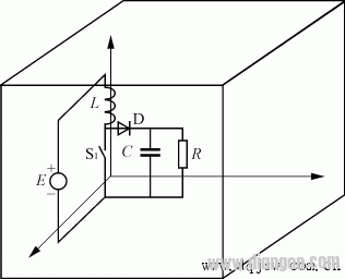
Figure 2 Distribution of Bosst circuits in three dimensions
It should be noted that the current phases of the different branches are not necessarily the same, which is especially important in the calculation of the magnetic field. The difference in phase is due to the delay of the interference from the source of the interference to the measurement point (also known as the hysteresis effect); another reason is that the characteristics of the component itself cause the phase to be different. For example, the current phase in the inductor is lagging behind other components. The phase lag caused by the hysteresis effect is the result of the signal frequency, and the effect is only obvious when the frequency is high (such as GHz level or higher); for power electronic devices, the frequency is relatively low, so the hysteresis effect is not very Big.
3 Several new electromagnetic interference suppression methods
Among the two types of interference generated by switching power supplies, conducted interference is transmitted through the power grid, causing serious interference to other electronic equipment, often causing more serious problems. Commonly used suppression methods are: buffer method, reduced coupling path method, and reduced parasitic element method. In recent years, with the stricter restrictions on electromagnetic interference of electronic equipment, some new suppression methods have emerged, mainly focusing on several aspects such as new control methods and design of new passive buffer circuits. The following are introduced separately.
3.1 New Control Method - Modulation Frequency Control
The interference is based on the switching frequency, and the energy of the interference is concentrated at these discrete switching frequency points, so it is difficult to meet the requirements for suppressing EMI. By distributing the energy modulation of the switching signal over a wide frequency band to produce a series of discrete sidebands, the interference spectrum can be spread out, and the interference energy is divided into small fractions distributed over these discrete frequency bands, making it easier to meet EMI standards. . The Modulated Frequency control is based on this principle to achieve the suppression of electromagnetic interference of the switching power supply. (Information source electrical automation technology network)
At first, people used randomized frequency control. The main idea was to add a random disturbance component to the control circuit to make the switch interval change irregularly. Then the switching noise spectrum changed from the original discrete spike noise to the continuous distribution noise. Its peak is greatly reduced. The specific method is that two different duty cycle pulses are generated by the pulse generator, and then the error signal generated by the voltage error amplifier is sampled and selected to generate a final control signal. The specific control waveform is shown in Figure 3(a).
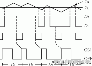
(a) Random frequency control principle waveform diagram
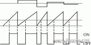
(b) Modulation frequency control principle waveform diagram
Figure 3 Two different frequency modulation waveforms
However, the random frequency control basically adopts the PWM control method when it is turned on, and adopts the random frequency when it is turned off, so the effect of modulating the interference energy is not very good, and the effect of suppressing the interference is not very satisfactory. The latest modulation frequency control solves these problems well. The principle is to modulate the main switching frequency to generate a series of sidebands around the main frequency band, thereby distributing the noise energy over a wide frequency band, reducing interference. The key to this control method is to modulate the frequency so that the switching energy is distributed in the range of the sideband, and the amplitude is affected by the modulation factor β (modulation coefficient β = Δf / fm, Δf is the interval between adjacent sidebands, fm is Modulation frequency), generally β is larger and the modulation effect is better, and its control waveform is as shown in Fig. 3(b).
Figure 4 shows a control circuit designed according to the modulation frequency principle. Various control methods can well suppress interference during turn-on and turn-off without affecting the operating characteristics of the converter.
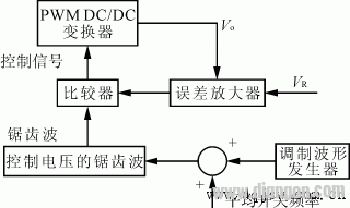
Figure 4 A typical modulation frequency control circuit
3.2 New Passive Buffer Circuit Design
The electromagnetic interference in the switching converter is generated at the time of switching of the switch. Taking a rectifier diode as an example, when turned on, its on-current not only causes a large amount of turn-on loss, but also generates a large di/dt, which causes electromagnetic interference. When turned off, the voltage across it rises rapidly, and there is a very high Large dv/dt, resulting in electromagnetic interference. The snubber circuit can not only suppress the di/dt at the time of turn-on, but also limit the dv/dt at the time of turn-off, and has the characteristics of simple circuit and low cost, and thus has been widely used. However, active auxiliary switches are often used in conventional snubber circuits. The circuit is complicated and difficult to control, and may cause higher voltage or current stress and reduce reliability. Therefore, many new passive buffers have emerged, which are summarized below.
3.2.1 Diode reverse recovery current suppression circuit
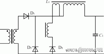
For the Boost circuit of Figure 5(a), after Q1 is turned on, D1 will be turned off. However, since the current on D1 is the operating current, it will drop to zero and its dv/dt will be high. The shutdown of D1 can only recover the current spike in the reverse direction, and the existing methods for suppressing the reverse recovery current of the diode are mostly applicable to a specific converter circuit, and only correspond to a certain input/output mode, and the applicability is poor. . Some people in foreign countries have proposed the circuit [6] of Figure 5(b), which can better solve this defect.
The key of Figure 5(b) is to connect an auxiliary diode (D2), a small auxiliary inductor (L2) in series with the partial coil of the main power inductor (L1), and then in parallel with the main diode (D1). The working principle is that when Q1 is turned on, the auxiliary circuit formed by the auxiliary inductor and the auxiliary diode is used for shunting, so that the current on the main diode D1 is reduced to zero and maintained until Q1 is turned off. Due to the effect of the inductor L2, the reverse recovery current on the auxiliary diode D2 is small and can be ignored.
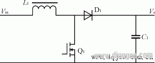
(a) Boost circuit
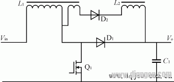
(b) Diode reverse recovery circuit
Figure 5 Boost circuit and its diode reverse recovery circuit
This method can be used in general converter circuits to limit the reverse recovery current of the main diode, and can also be used for the recovery current suppression of the input and output rectifier diodes. Figure 6 is an example of such an application. This technology can be applied to general power supply circuits to effectively suppress reverse recovery peak currents, reduce EMI, and reduce losses and improve efficiency.
(a) Input rectifier circuit
(b) Output rectifier circuit
Figure 6 input and output rectifier diode reverse recovery current suppression circuit
3.2.2 Lossless snubber circuit
In the converter circuit, when the main diode is reversely restored, it will cause a large current and voltage stress on the switch tube, causing a large power consumption, which is likely to cause damage to the device. In order to suppress this reverse recovery current and reduce the loss, a lossless buffer circuit [5] is proposed, as shown in Fig. 7.
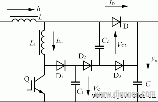
Figure 7 lossless snubber circuit
The main working principle is that the di/dt stress when the main switch Q is turned on and the dv/dt stress at the time of turn-off are respectively limited by L1 and C1, and the mutual resonance and energy conversion between L1, C1 and C2 are used to realize the pair. The main diode D reverses the recovery of the current, which greatly reduces the switching loss and EMI. Not only that, because the energy on C1 is transferred to C2 when it is turned on, the energy on C2 and L1 is transferred to the load when it is turned off. This snubber circuit has low loss and high efficiency.
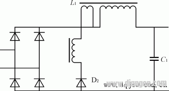
3.2.3 Passive compensation technology
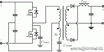
The conventional common mode interference suppression circuit is shown in FIG. In order to maintain the leakage current flowing into the ground through the filter capacitor Cy in a safe range, the value of Cy is small, and the corresponding choke coil LCM becomes large, especially since the LCM transmits all the power, its loss, volume and weight will be Become bigger. By applying passive compensation technology, the common mode interference of the circuit can be better suppressed without affecting the operation of the main circuit, and the LCM can be reduced and the cost can be saved.

Figure 8 Common mode interference filter
Since the common mode interference is generated by the dv/dt of the parasitic capacitance of the switching device at high frequencies, an additional transformer winding is used to generate a 180° reverse voltage across the compensation capacitor, and the resulting compensation current is parasitic. The interference current on the capacitor is superimposed to eliminate interference. This is the principle of passive compensation.
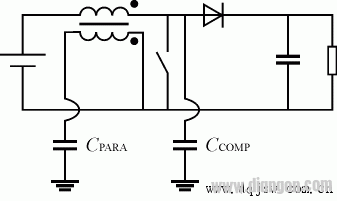
Figure 9(a) shows an isolated half-bridge circuit incorporating a compensation circuit. Since the half-bridge and full-bridge circuits are often used in high-power applications, the filter inductor LCM is large, so the compensation effect will be more obvious. The circuit adds a compensation coil Nc to the transformer, the number of turns is the same as the primary winding; the size of the compensation capacitor CCOMP is the same as the parasitic capacitance CPARA. In this way, Nc during operation causes CCOMP to generate a compensation current of the same magnitude and opposite direction as the interference current on CPARA, and the interference current is eliminated after the superposition. The compensation coil does not flow all the power, only the interference current is transmitted, and the compensation circuit is very simple.
Similarly, for the forward circuit of Figure 9(b), compensation can be achieved more conveniently with its own magnetic reset coil. Passive compensation techniques can also be applied to non-isolated converter circuits, as shown in Figure 10, the principle is the same.
(b) Forward circuit with compensation circuit
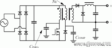
(a) Isolated half-bridge circuit with compensation circuit
Figure 9 two passive compensation circuits
(a) Boost circuit
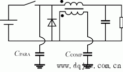
(b) Buck circuit
Figure 10 Non-isolated Boost, Buck circuit with compensation circuit
It should be noted that the passive compensation technology has certain application conditions, which are affected by factors such as switching current, voltage rise and fall time, and transformer structure, especially when the line-to-line coupling capacitance of the transformer is much larger than the parasitic capacitance. The current enters the earth directly without the compensation coil, and the suppression effect is not ideal at this time.
4 Conclusion
There are many sources of noise, such as external interference, mechanical vibration, improper circuit design, improper component selection, and unreasonable structural layout or wiring. In switching converters, the RF energy generated by the power transistors and diodes during the on-off process is one of the main sources of interference. Due to the high frequency, or directly radiated to the space (radiation interference) in the form of electromagnetic energy, or transmitted along the input and output wires in the form of interference current (conducted interference), the latter is more harmful.
Switching power supply technology is a comprehensive technology that uses advanced semiconductor circuit design techniques, magnetic materials, inductive component technology, and switching device technology to effectively reduce and suppress EMI. At present, switching power supplies have been increasingly widely used in various control devices, communication devices, and household appliances. The electromagnetic interference problem and electromagnetic compatibility with other electronic devices have become a hot spot of concern, and electromagnetic interference and related in the future. The problem is bound to get more research.
Stereo Audio Cable, Audio cable, stereo cable, aux plug cable
Stereo Audio Cable, Audio cable, stereo cable, aux plug cable
Ningbo Multitasking Electronic Co.,Ltd , https://www.smartmultesic.com