
Direct frequency synthesis technology is actually a digital synthesis technology that converts stored waveform data to a desired analog signal through a high-speed D/A converter through a specific algorithm. The basic principle diagram is shown in Figure 1.
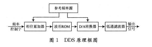
Can be seen from Figure 1, which is mainly composed of standard reference frequency source, phase accumulator, waveform memory, digital / analog converter and other parts. Among them, the reference frequency source is generally a highly stable crystal oscillator, and its output signal is used for synchronous operation of various components in the DDS. When the frequency synthesizer works normally, the phase accumulator continuously accumulates the phase increments under the control of a standard frequency reference source (the frequency control word K determines the phase increment thereof) when the phase accumulator is full. When there is an amount, an overflow occurs, completing a periodic action, that is, a frequency cycle of the synthesized signal. The output address of the accumulator addresses the waveform ROM to convert the sample values ​​stored in the phase accumulator into a corresponding sine wave amplitude sequence. The digital quantity is converted into an analog quantity by high-speed D/A conversion, further smoothed by a low-pass filter, and the out-of-band spurs are filtered out to obtain a desired waveform.
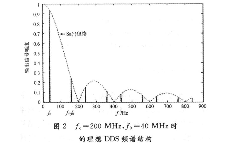
2. Analysis of sinusoidal signals by DDSThe output spectrum of an ideal DDS is the spectrum that the system outputs when there is no phase rounding error, amplitude quantization error, and DAC error. At this time, the entire DDS system is equivalent to the ideal sample-and-hold circuit. The spectral structure of the output signal is a set of discrete spectral lines with the Sa(•) function as the envelope, as shown in Figure 2 (selected fc=200 MHz, fo=40 MHz), only at f=nfc±fO= There are discrete lines at (n±K/2N)fc.
The AD9854 digital synthesizer is a highly integrated DDS device from AD. It integrates a dual 48-bit frequency accumulator, dual 48-bit phase accumulators, a sine/cosine waveform table, and dual 12-bit orthogonal digital-to-analog converters. A 12-bit digital multiplier, a programmable reference clock multiplier, and a modulation and control circuit can implement frequency modulation, phase modulation, programmable amplitude modulation, and I, Q two-way quadrature modulation and other functions on the microcontroller. When the AD9854 is used as an accurate clock source, it can produce high stability, sine and cosine output with a frequency-phase-to-amplitude programmable. Its main features are:
The operating frequency is high and its operating frequency is up to 300 MHz. Its circuit configuration allows the generation of simultaneous output signals with a frequency up to 150 MHz. Phase truncation to 17 bits guarantees excellent spurious-free signal dynamic range (SFDR).
The high frequency resolution of its innovative high-speed DDS core provides 48-bit frequency resolution (1 μHz regulation resolution at 300 MHz SYSCLK).
Programmable Reference Clock Multiplier The AD9854 programmable 4 & 20; TI's REFCLK multiplier circuit internally generates a 300 MHz system clock from a low frequency external reference clock, saving the user's cost and reducing the system's clock source. Difficulty.
Integrated high-performance DACs internally Two 12-b/300-MHz DACs meet the signal-to-noise ratio (SNR) of the output signal.
Simple high-speed serial and parallel data interface parallel port data transfer rate reaches 100 MHz, serial port also has 10 MHz speed, and the minimum frequency conversion time can reach 10 ns.
There are five programmable operating modes for multiple operating modes: single-tone mode, non- ramp-up FSK, ramp-up FSK, linear frequency modulation, and BPSK, which can be switched according to different needs during use.
STM32 AD9854 DDS module debuggingRecently, because the game needed to produce its own signal source, the AD9854 DDS module was selected on a certain treasure. The internal structure was not introduced, and the manual was available. The module can generate I, Q two orthogonal output signals, that is, one way sine one cosine signal, and one comparator output signal, that is square wave signal. If you do not require the output signal amplitude can also choose AD9851 this module is quite classic. The debugging method is similar to that of the 9854. I use a serial communication mode, which saves IO ports. First, the AD9854 is initialized and the code is written according to the timing diagram in the manual. In the serial mode, the S/P must be connected to the low level, and the output of the other function IO ports is the push-pull output mode and the pull-up input mode. Initialization procedure:
[html] view plaincopy"span style="font-size:18px;""void AD9854_Init_S(void)
{
AD9854_M_Reset_H();
AD9854_SP_L();
AD9854_SCLK_L();
AD9854_SDIO_L();
AD9854_IO_UD_CLK_L();
AD9854_CS_H();
AD9854_IO_Reset_H();
Delay_int(10);
AD9854_M_Reset_L();
Delay_int(10);
DATA[3]=0X00;
DATA[2]=0X4a; //10 multiplier
DATA[1]=0X00;
DATA[0]=0X60;
AD9854_Send_Data(0x07,DATA);
}"/span"
Secondly, write the value to the corresponding address of the register, the serial communication address corresponds to 0x00~0x0B, and the address and serial address of the parallel communication are different from the serial connection. For details, refer to the manual. For simple frequency amplitude control, the address of interest is only 0x02 (I channel frequency control address) 0x03 (Q channel frequency control address) 0x07 (frequency multiplier address) 0x08 (I channel amplitude control address) 0x09 (Q channel amplitude control address).
The register write value is first written low and the write high.
0X07 addresses a total of 4 bytes, the write value is DATA[3]=0X00; DATA[2]=0X4a; DATA[1]=0X00; DATA[0]=0X60; if only the multiplier factor is modified, only the DATA needs to be modified. The value of [2] (range 4-20 times, actual maximum 10 times frequency), you can modify the value of the corresponding address in the other function comparison manual. 0x02 addresses a total of 6 bytes, 100M corresponding frequency word is DATA[0]=55; DATA[4]=55; DATA[3]=55; DATA[2]=55; DATA[1]=55; DATA[ 0]=55; 1M=940000000000 after converting to hexadecimal; after writing the value, it only needs to shift to the corresponding address to facilitate frequency stepping and sweep function afterwards. 0x03 same. Someone will ask: Why do you need to set the frequency multiplier here? With respect to the multiplication factor, if the output frequency is relatively high and the multiplication coefficient is relatively small, the output waveform will be distorted, so the multiplication factor is set according to the frequency of your output. The frequency setting function code is as follows:
[html] view plaincopy" span style="font-size:18px;""void AD9854_SetFre(long long fre) //Maximum input is 2^48
{
DATA[5]=(u8)(freâ€â€40);
DATA[4]=(u8)(freâ€â€32);
DATA[3]=(u8)(freâ€â€24);
DATA[2]=(u8)(freâ€â€16);
DATA[1]=(u8)(freâ€â€8);
DATA[0]=(u8)fre;
AD9854_Send_Data(0x02,DATA);
AD9854_Send_Data(0x03,DATA);
}//If I, Q output different frequency, 0X03 input value can redefine an array. "/span"
0x08 address of a total of 2 bytes, the measured 10mV = 450; amplitude setting function code is as follows:
[html] view plain copyvoid AD9854_SetSine(u16 Shape) // maximum input 2^16
{
Unsigned char A[2]={0};
A[1]=Shapeâ€â€8;
A[0]=Shape&0XFF;
AD9854_Send_Data(0x08,A);
AD9854_Send_Data(0x09,A);
}//If two different amplitude outputs are required, refer to the above frequency control.
After these steps are completed, the connection should output the signal you want, but there may be a constant output of a certain frequency, and there are many steps in the waveform is not smooth, no matter how you modify the multiplier coefficient, the output will not change, modify the frequency The word output waveform will not change as you would expect. This problem I have spent a whole few days, is really helpless, requires an external 5V power supply, just started using the computer USB power supply that led to a small input current, and later switched to a 5V power supply, current 2A, or no improvement, The GND on the 9854 module is the same as the GND of the microcontroller. Later it was discovered that there was a voltage difference between the two GNDs, and no real common ground was achieved, causing the chip to malfunction.
Solution: When the external 5V power supply is connected to the 3.3V power supply on the 9854 module, it is also connected to the 3.3V power supply on the single-chip microcomputer. This should constitute a loop, and GND can realize the true common ground and solve the problem. 9854 this module is still very easy to use, initialization timing is no problem, as long as the corresponding address write value can achieve the output you want. For parallel communication, the timing is correct, and the value of the serial address is slightly different. It is not difficult to refer to the manual.
Multi-core cpu is more and more popular, people are used to take dual core processors laptop before. However, Quad Core Laptop is becoming selling like a hot cake nowadays. You can find Quad Core Processor Laptop at our store, like I3 Quad Core Laptop,I7 Quad Core Laptop, I5 Quad Core Laptop, intel celeron J4125 or N5095 15.6 Inch Laptop, even N4120 quad core 14 Inch Laptop, etc. Therefore, you can just share the parameters prefer, like size, cpu, ram, rom, gpu, application scenarios, thus save much time to get a win-win solution.
Do you know the reason why more people choose quad core device? The core reason is that heavier tasks people need to finish at a higher speed than before. Nowadays quick rhythm is becoming the main style in city even everyone is eager to downshifting. So more powerful laptop, computer, mobile phone is a trend, though most functions never are used in lifetime.
15.6 inch Gaming Laptop or 14 Inch Gaming Laptop is becoming the most popular level at the market.
Quad Core Laptop,I3 Quad Core Laptop,I7 Quad Core Laptop,I5 Quad Core Laptop,Quad Core Processor Laptop
Henan Shuyi Electronics Co., Ltd. , https://www.shuyioemelectronics.com