
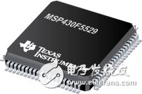
The MSP430F5529 is the latest generation of ultra-low-power microcontrollers with integrated USB that can be used in applications such as energy harvesting, wireless sensing, and automatic meter reading. It is one of the lowest power consumption microcontrollers. MSP430F5529 development board (MSP-EXP430F5529) is the development platform of MSP430F5529 microcontroller, consisting of power selection switch, RF interface, microSD card slot, MSP430F5529 chip and lead pin, USB interface, JTAG emulation interface, gear potentiometer, capacitive touch button , LED, button, EZ-FET built-in emulator, 102x64 dot matrix LCD and three-axis accelerometer. The development board connects the I/O pins to facilitate the user's experimental operation. It can be used for scientific research and development, as well as experimental teaching, curriculum design, graduation design, etc., providing a good experimental development environment for teachers and students. It is also a good platform for the majority of electronic enthusiasts to learn and develop MSP430 series MCUs.
There are two types of timers in the MSP430F5529. There are 3 TImer_A timers and 1 TImer_B timer. The number of capture/comparators provided in each register is named TImer0_A (with 5 capture comparators). , TImer1_A (3), Timer2_A (3), Timer0_B (7).
Timer_A timer 3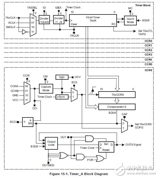
Timer A is a sixteen-bit timing (addition and subtraction) counter that is combined with the capture/compare register. Timer A supports multiple capture/compare, PWM output and internal timing with extended interrupt function, which can be generated by a timer overflow or by a capture/compare register.
Feature introduction:
1. Asynchronous 16-bit timer/counter in four operating modes
2, its own clock source can be configured
3. Up to 5 configurable capture/compare registers (CCR)
4, configurable PWM output
5, asynchronous input and output latch
6. Interrupt vector register for fast response to all Timer_A interrupts
TASSELx: Clock source selection. Try not to select the TASSEL0-TACLK external clock source, because if TACLK and CPU clock are not synchronized, it is easy to go wrong. (TA0CLK is connected to P1.0 pin)
00 TACLK 01 ACLK 10 SMCLK 11 ~TACLK
IDx: The first crossover control. ID0-1 frequency division; ID1-2 frequency division; ID2-4 frequency division; ID3-8 frequency division
MC: Work mode control. (It is recommended to stop the timer (interrupt enable, interrupt flag, TACLR exception) before modifying the timer operation mode to avoid unknown misoperation.)
00 Stop mode: Timer stop 01 Increase mode: Timer counts to TACCR0 10 Continuous mode, timer counts to 0FFFH 11 Increase/decrease mode: Timer counts up to TACCR0 and then counts down to 0000H
TACLR: Timer clear bit. This bit will reset the TA register, clock division and count direction. The TACLR bit will be automatically reset and set to 0.
TAIE: Timer Interrupt Enable 0: Interrupt Disable 1: Interrupt Enable
TAIFG: Interrupt flag bit 0: No interrupt occurs 1: Interrupt pending
Count value storage register TAR
1, obviously, the maximum storage count value is 0xFFFFh;
2, (similar to 51 MCU) can be used to store an initial value, and then select continuous mode. This is continuously filled and then manually filled to achieve accurate timing results;
3, the default is 0, and the register can be directly assigned;
Extension register TAEX0
Quite simply, this register is used to control the secondary divide of the clock source.
The lower 3 of this register is defined as TAIDEX:000-111, which means 1-8 frequency division respectively.
Capture/Compare Register TACCR0-TACCR4 (5 total)
In the comparison mode, it is used to set the final value of the count;
Capture mode is used to store captured TAR values ​​into TACCRx.
Detailed explanation of the four working modes of MC control
MC=0 stop mode
This is the default mode of the system and the timer counter is disabled.
MC=1 increase mode
1. It is strictly forbidden to start counting from 0xffff in this mode;
2, note that from 0 to TACCR0, actually recorded TACCR0 + 1 number;
3. After counting TACCR0, it will return to 0 to restart counting;
4. If the value of TAR is greater than TACCR0, then it will start counting from 0 at this time;
5. When the timer counts to the value of TACCR0, the interrupt flag CCIFG bit (described later) is set. When the timer returns 0 from TACCR0, the TAIFG interrupt flag is set;
6. Modify TACCR0 while the timer is running. If the new period value is greater than or equal to the old period value, or greater than the current timer count value, the timer will immediately start executing the new cycle count. If the new period is less than the current count value, the timer returns to zero. However, there will be an extra count before returning to zero.
MC=2 continuous mode
In continuous mode, the timer repeats counting to 0FFFFH and then increments again from 0 (unless the initial value is reloaded each time). When the timer goes from 0FFFFH to 0, the TAIFG interrupt flag is set.
Application: Use the capture/comparator to generate the required time interval in continuous mode. The principle is: the count is always on, the first count value is stored in the trap TACCRX, and each time the trap counts TACCRX, an interrupt flag is generated. We can write a calculated next one in the interrupt service function. The final value of the count, so that infinite calculations and interrupts, then the trap will produce a stable sequence of time intervals. (Actually, it doesn't matter if you don't understand it. Even if you understand it, it's not easy to use, because it's too complicated to calculate and it doesn't work well.)
MC=3 increase and decrease mode (usually used to generate PWM waves)
1. In this mode, the counting direction is fixed, that is, the timer is restarted after the timer is stopped, and it starts counting along the counting direction and value at the time of stopping. If you don't want this, you need to set the TACLR to clear the direction. The TACLR bit also clears the value of the TAR and the clock division of the timer.
2. When the timer is running, change the value of TACCR0. If it is in the down count, the timer will continue to decrease to 0, and the new cycle will start after decreasing to 0. If it is in the up count state, the new period is greater than or equal to the original period, or larger than the current count value, the timer will count up to the new period; if the new period is less than the original period, the timer will immediately start counting down, however, One more number is counted before the timer starts counting down.
Timer_B timer 1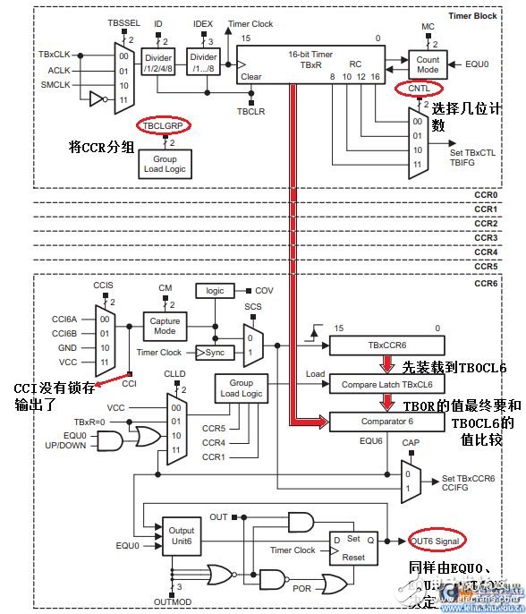
Introduction to Timer B
Timer_B timer feature :
(1) 16-bit synchronous timing/counting, 4 working modes are optional, and 4 medium lengths are optional;
(2) Optional configurable clock source;
(3) Up to 7 capture/compare registers;
(4) Configurable PWM output;
(5) Double buffered compare register with synchronous loading;
Comparison with timer A (same point and difference)
(1) The counting length of TB can be selected (8, 10, 12, 16 BITS), while the TA has only 16 bits;
(2) The TB0CCRn registers are double buffered and can be grouped;
(3) All TB outputs can be set to a high impedance state;
(4) TB does not have SCCI, that is, the capture input signal CCI is not latched;
(6) Interrupt vector for fast decoding;
Timer0_B register introduction and setting
Declaration: All registers also support word and byte operations
All registers are initialized to 0x0000
TB control register TB0CTL (most common and most basic) (a little different from TA)
Rw-(0) means the default read and write is 0
TBCLGGRP: TB0CLn group control
00: Each TB0CLn is used independently
01: TB0CL1+TB0CL2 as a group (CLLD bits of TB0CCR1 control the entire group of data updates)
TB0CL3+TB0CL4 as a group (CLLD bits of TB0CCR3 control the entire group of data updates)
TB0CL5+TB0CL6 as a group (CLLD bits of TB0CCR5 control the entire group of data updates)
10: TB0CL1, 2, 3 group, (CLLD bit of TB0CCR1 controls the entire group of data updates)
TB0CL4, 5, 6 group, (CLLD bit of TB0CCR4 controls the entire group of data updates)
11: TB0CL0, 1, 2, 3, 4, 5, 6 are integrated into one group.
(CLLD bit of TB0CCR1 controls the entire set of data updates)
CNTL: Counter length control
00 16 bits, that is, up to 0FFFFh
01 12-bit, that is, up to 0FFFh
10 10 digits, that is, up to 03FFh
11 8 bits, that is, up to 0FFh
TBSSEL : Clock source selection. Try not to select the TACLK external clock source, because if TACLK and CPU clock are not synchronized, it is easy to go wrong. (TB0CLK is connected to P7.7 pin)
00 TBCLK
01 ACLK
10 SMCLK
11 ~TBCLK
ID: The first frequency division control. ID0-1 frequency division; ID1-2 frequency division; ID2-4 frequency division; ID3-8 frequency division
MC: Work mode control. (It is recommended to stop the timer (interrupt enable, interrupt flag, TACLR exception) before modifying the timer operation mode to avoid unknown misoperation.) (same as TA)
00 stop mode: timer stop
01 Increase mode: The timer counts to TB0CCR0
10 continuous mode, the timer counts to 0FFFH (16 bits)...12 bits, 10 bits...
11 increase and decrease mode: the timer counts up to TB0CCR0 and then counts down to 0000H
TBCLR: Timer clear bit. This bit will reset the TA register, clock division and count direction.
The TACLR bit will be automatically reset and set to 0.
TBIE: Timer Interrupt Enable
0: Interrupt prohibition
1: Interrupt allowed
TBIFG: Interrupt flag
0: no interruption occurred
1: There is an interrupt pending
Count value storage register TB0R
Expansion register TBEX0
Quite simply, this register is used to control the secondary divide of the clock source.
The lower 3 of this register is defined as TBIDEX:000-111, which means 1-8 frequency division respectively.
Capture/Compare Registers TBCCR0-TBCCR6 (7 total)
In the comparison mode, it is used to set the final value of the count;
Capture mode is used to store captured TBR values ​​into TBCCRx.
Capture/compare control register TB0CCTL0-TB0CCTL6:
CM: Capture mode setting 00 does not capture
01 rising edge capture
10 falling edge capture
11 rising and falling edges are captured
CCIS: Capture Source Selection 00 CCIxA
01 CCIxB
10 GND
11 VCC
SCS: Synchronize the capture source and set whether to synchronize with the clock
0 asynchronous capture
1 sync capture
CLLD: Compare register buffer load mode selection.
00 TB0CCRn value (when changed) is immediately loaded to TB0CLn
01 Load when the value of TB0R counts to 0
10 In the incremental mode or continuous mode, when the TBR0 value counts to 0, it is loaded;
In the increase/decrease mode, when TBR0 counts to TBCL0, it starts loading;
11 When TBR0 counts to TBCL0, it starts loading;
CAP: 0-Compare Mode 1 - Capture Mode
OUTMOD: Output mode control bit. Same as TA
CCIE: Interrupt Enable, this bit allows the corresponding CCIFG flag to interrupt the request.
0-interrupt disable 1 - interrupt enable
CCI: capture comparison input, the selected input signal can be read by this bit
OUT : For output mode 0, this bit directly controls the output state.
0-output low level 1-output high level
COV: Capture overflow bit. This bit indicates a capture overflow is issued and the COV must be reset by software.
0 - no capture overflow occurred 1 - there is a capture overflow
CCIFG: Capture compare interrupt flag bit.
0 - no interrupt pending 1 - interrupt pending
Interrupt vector register TB0IV
Like TAIV, it stores a number.
Difference between TB and TA
No longer latched the CCI signal
When TA is used as a trap, CCI is the capture signal, and then CCI is latched and output as SCCI;
However, TB is not latched. This means that the input signal can only be viewed from the CCI bit.
The number of counts is adjustable (in fact, it doesn't matter, you can do it for 16 people)
TA's count value register TAR can only be 16 bits (0XFFFFh);
The TB count value register TBR can be selected to be 16, 12, 10, 8 bits;
Two-stage buffer comparator (comparative mode)
In TA, we write the value to be compared in TACCRn, and then compare the count value in TAR with TACCRn. If they are equal, the corresponding flag will be set.
In the TB, there is not only TB0CCRn, but also a second-level buffer TB0CLn. TB0CLn cannot be operated directly, its value can only be derived from TB0CCRn. When counting, the count value in TB0R is not compared with TB0CCRn, but is compared with TB0CLn.
The secondary buffer is to prevent us from affecting the count when we modify the value of TB0CCRn. Because the counter is not directly compared to TB0CCRn, but TB0CCRn assigns the value to TB0CLn, which is compared to TB0R by TB0CLn. So there is the CLLD bit control compare register buffer load mode: (when rewriting the number to TB0CCRn)
The value of 00 TB0CCRn is immediately loaded into TB0CLn
01 Load when the value of TB0R counts to 0
10 In the incremental mode or continuous mode, when the TBR0 value counts to 0, it is loaded;
In the increase/decrease mode, when TBR0 counts to TBCL0, it starts loading;
11 When TBR0 counts to TBCL0, it starts loading;
Comparators can be grouped
TA does not have a secondary buffer register, and the original TACCRn can only be used alone.
For TB:
TBCLGGRP: TB0CLn secondary buffer register grouping control
00: Each TB0CLn is used independently
01: TB0CL1+TB0CL2 as a group (CLLD bits of TB0CCR1 control the entire group of data updates)
TB0CL3+TB0CL4 as a group (CLLD bits of TB0CCR3 control the entire group of data updates)
TB0CL5+TB0CL6 as a group (CLLD bits of TB0CCR5 control the entire group of data updates)
10: TB0CL1, 2, 3 group, (CLLD bit of TB0CCR1 controls the entire group of data updates)
TB0CL4, 5, 6 group, (CLLD bit of TB0CCR4 controls the entire group of data updates)
11: TB0CL0, 1, 2, 3, 4, 5, 6 are integrated into one group.
(CLLD bit of TB0CCR1 controls the entire set of data updates)
The so-called grouping is that the data of the group should be updated at the same time.
Take the group of TB0CL1, 2, and 3 in 10 mode as an example:
The CLLD in TB0CCTL1 is set to 01. When TB0R counts to 0, TB0CCR1 will load (update) the value into TB0CL2, and TB0CCR2 will load (update) the value into TB0CL2, and TB0CCR3 will also load the value ( Update) to TB0CL3. No matter how many values ​​in TB0CCRn have changed, they only update TB0CLn at the same time.
You can look for top sell products here.Our factory is located in Guangzhou, China's "leather capital", which will be more affordable in terms of the price of goods.
We employ the most creative designers and tech brilliant engineers to make the best cases. We believe our high-quality products with competitive prices will satisfy your needs.
The productive process :
Make the Products Mould –Cutting the fabric –Do the half products – Finish products – Cleaning –QC- Package – Shippment .
TOP Sell Items,Ysue TOP Sell products,Hot selling products in store,customized leather cases
Ysure Leather case 24/7 Support : 86 13430343455 , https://www.ysurecase.com