
Discuss the structure and application of LCoS display, and give the design method of LCoS display chip and its actual design result. The LCoS display is a reflective liquid crystal display. The peripheral driver and active pixel matrix are fabricated on a single crystal silicon substrate using CMOS technology, and the wafer is used as a substrate liquid crystal cell, thus having a small size and high display resolution. characteristic.
1 LCoS display chip - a new type of SoC chip
When it comes to liquid crystal displays, people think of LCD monitors for notebook computers or large-screen plasma displays. The emerging and exciting LCoS is the LCD display technology made on monocrystalline silicon. LCoS display is a new type of reflective display. It is a high-tech product combining semiconductor VLSI technology and liquid crystal display technology. Its display chip has a diagonal size of 18mm. Because LCoS can be mass-produced using conventional CMOS technology, and can be further miniaturized with the development of semiconductor technology, while improving resolution, LCoS displays will have low power consumption, miniature size, ultra-light weight, etc., so in personal portable display applications The aspect is very advantageous, especially the power consumption is much lower than many active matrix liquid crystal displays (AMLCDs), and the production cost is expected to be comparable to that of a cathode ray tube (CRT).
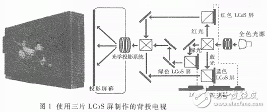
Although LCoS displays usually have a nail size and the corresponding pixels are so small that they are not directly visible to the naked eye, LCoS displays are equipped with a wide variety of Optic Engines for magnification: one is direct Projecting onto the retina to form an enlarged virtual image, thereby producing a personal virtual imaging flat display technology; the other is to use the screen projection to form a magnified real image, as shown in FIG. LCoS display technology led to the birth of a new class of large-screen flat panel display devices.
The monocrystalline silicon backplane (LCoS display chip), a key component of the core of the LCoS display technology, is a versatile, multi-structure system-on-a-chip (SoC) in which the entire display system is integrated on a wafer of approximately 18 mm. However, the design of SoC-based chips must take into account the various conditions of the entire system. Because of this design, SoC-based chips can achieve higher performance system specifications under the same process technology compared to display systems combined with separate ICs. It can be expected that the application prospect of the new generation of liquid crystal displays designed and produced by the system chip will be very broad.
2 LCoS display
LCoS displays are generally divided into two broad categories: transmissive and reflective. Although their geometric optics are completely different in principle, they can selectively modulate the light from the external source to form an image. The transmissive type firstly designs and fabricates the driving control circuit on the wafer, and then separates the die by a lift-off technique or an anisotropic etching technique, and adheres to the transparent substrate to form a microdisplay. chip. Such a clever design is based on the use of high-quality electrical properties of single crystal silicon, on the other hand is the use of mature IC design and manufacturing technology. The reflective type is to directly fabricate a driving circuit and a display matrix circuit on a wafer, and then package the liquid crystal material as a substrate to form a flat panel display similar to a conventional LCD (Liquid Crystal Display) structure. Therefore, conventional IP technology can be directly used to design and manufacture silicon-based liquid crystal displays.
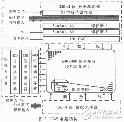
Figure 2 is a schematic diagram of a reflective LCoS (VGA resolution, timing colorization) circuit designed by the author using the Cadence EDA tool with a 0.6 μm n-well four-layer metal CMOS process. The circuit can be divided into a row scan driver, a column data input driver (including the DAC circuit), and a display driver matrix (active NMOS matrix).
In the column data input driver, the serial input multi-bit digital video signal is sequentially stored in the digital latch by the action of the shift register, and then, under the action of the same read signal, the line scan signal is matched and input to each column at the same time. The digital-to-analog converter (DAC), after which the output analog voltage signal is applied to the pixels, so one frame of image will be transmitted to all columns one line at a time.
In a row scan driver, the row scan signal is applied through another set of shift registers to produce a progressive scan signal that is synchronized with the digital video signal.
Each of the active display drive matrix includes a pixel switch (NMOS transistor), a storage capacitor, and an aluminum reflective electrode thereon. The NMOS transistor controls the column data line to charge the liquid crystal pixel, and the charge charge in the storage capacitor establishes a voltage difference relative to the control electrode. Since the liquid crystal material itself also has a capacitance and is charged in the orientation of the molecules, when a certain amount of charge accumulates on the pixels, the liquid crystal will be oriented according to the applied electric field. The reorientation of the liquid crystal molecules causes a change in the liquid crystal capacitance, which changes the voltage applied to the pixels. In order to solve this problem, a larger storage capacitor is required.
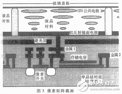
The cross section of the pixel is shown in Fig. 3. Four layers of metal are used for the scanning line, the data line, the dark layer and the aluminum mirror electrode. The scan line controls the gate of the NMOS transistor (pixel switch), and the signal on the data line is driven to the pixel when the NMOS is turned on. The transistor drain, storage capacitor and mirror electrode are electrically conductive. A 1 μm thick liquid crystal pad was formed on the top of the silicon back sheet to determine the cell gap.
The entire silicon backplane is completed on a conventional IC chip production line. On the processed LCoS display chip, the alignment layer is covered, the sealant is applied, the glass cover plate to which the ITO electrode is attached is adhered, and finally the liquid crystal material is poured into the liquid crystal cell to form an LCoS display. Although the area of ​​the LCoS display chip is relatively large, most of them are pixel arrays, and the transistor density is low, so that a high yield can be obtained. The use of modern IC manufacturing technology to produce LCoS displays is easy to use and is a cost-effective way to create high-resolution LCD displays.
3 chip power analysis
Power loss is an important factor in the implementation of integrated circuits, and the main feature of CMOS circuits is low power consumption. Since the pixel size on the LCoS chip is very small (7 to 20 μm), the process of fabricating the corresponding micro-filter (microfiLTEr) is complicated and costly. Colorless display is usually performed on a single LCoS chip using a time-mixed color mode (timing colorization). On the surface, the LCoS chip with timing color mode requires that the frame rate is more than three times that of the normal VGA display to refresh the screen. It seems that the power consumption will increase many times, but this is not the case. In the actual circuit structure of Figure 2, we designed a row latch. In this way, the image signal of each field can be input into the pixel display matrix by using the progressive writing method. The video string-to-row conversion shift register in the vertical data driver operates at approximately 25 MHz, and most other circuits do not exceed 300 kHz. The power consumption of the LCoS chip includes the following three parts: (1) Static power consumption Ps. The dc circuit is generally negligible due to the DC power dissipation caused by the reverse leakage current.
(2) Dynamic power consumption PD. It mainly refers to the AC power consumption generated by charging and discharging pixels (capacitors) per row when image signals are written line by line.
(3) Field inversion power consumption PF. The upper cover electrode is used for the power consumption required for periodic electric field inversion.
Combining the above three power consumptions, the total power consumption is
P=Ps+PD+PF≈PD+PF(1)
The digital circuit transient power estimation formula can be used to obtain:
P=CL fc VDD2 (2)
Here, the capacitance CP of each pixel is about 0.2 pF.
The capacitance of each row of pixels is:
Crow=640&TImes;CP=128pF (3)
The capacitance per pixel of the screen is:
Cpanel=480&TImes;Crow=61.44nF (4)
In addition, it is known that the progressive write frequency is close to 300 kHz, the field inversion frequency is 150 Hz, and VDD = 5 V. These values ​​are substituted into (1) with equations (2), (3), and (4) to obtain the power consumption of the LCoS chip. estimated value:
P=Crow f line VDD2+Cpanel f field VDD 2≈1.2nW, it can be seen that LCoS display is indeed a low power device.
The LCoS chip designed and fabricated by the 0.6μM CMOS process has a pixel cutoff of 12μm; the pixel drive matrix has an area of ​​(640 & TImes; 12) μm (480 × 12) μm = 7.68mm × 5.68mm × 5.76mm. Considering the need to reserve the glue line encapsulation area of ​​the liquid crystal cell, the size of the entire LCoS display chip is: 11.0 mm × 9.4 mm, and the diagonal is about 15 mm.
4 LCoS chip development strategy and modern EDA technology
From the previous analysis of the device structure and the working mode of the whole chip, the LCoS chip is a complex digital-analog hybrid circuit chip. The complexity of this type of circuit not only requires the same production line to be compatible with both digital and film-like IC production processes, but more importantly, how to accurately and quickly design LCoS display chips for market needs. It is relatively easy to implement a modern semiconductor processing factory with a certain scale of the former, and the latter is largely procedurally determined by the EDA design platform to be adopted.
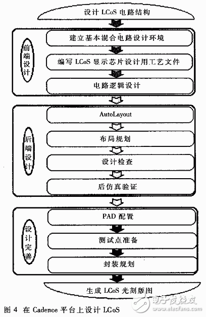
The so-called EDA refers to the electronic CAD general software package developed by computer as the working platform and the latest achievements of application electronic technology, computer technology and intelligent technology. It can mainly assist in the design work of three aspects: IC design and electronic circuit design. And PCB design. We will use the Cadence EDA design tool with full custom design capabilities to design the layout of the LCoS chip in accordance with the "top-down" rules. Design begins with behavioral level, first determining the functionality, performance, allowable chip area, and cost of the LCoS chip. According to the structural design, the subsystems that are as simple as possible are differentiated. Then the logic relationship between the subsystems is converted into a circuit diagram, circuit logic design and circuit simulation. During this period, the standard 5V-0.6μm-CMOS process design rules are followed, and the basic cell library of the LCoS chip is developed by the full customization method. Finally, the entire LCoS chip layout is synthesized according to the semi-custom design flow.
5 Designing the LCoS chip layout on the CADENCE platform
According to the processing conditions of China's microelectronics industry, Cadence software with rich EDA tools was selected, and a set of 0.6μm process LCoS chip layout was established, including circuit symbol library, circuit design library, cell version library and its layout and layout. Phanton library and simulation library etc. The main design flow is shown in Figure 4.
First determine the design and choose the appropriate CMOS process to implement the solution. The versatile designer designs the circuit schematic based on the specific CMOS component parameters. The first simulation is then performed, including logic simulation of digital circuits, fault analysis, AC/DC analysis of analog circuits, and transient analysis. When the LCoS chip circuit is being simulated, it must be supported by the component model library. The analog input and output waveforms on the computer replace the signal source and oscilloscope in the actual circuit debugging. This simulation is mainly to verify the correctness of the design in terms of function.
EDA technology enables LCoS designers to fully understand the functional and physical characteristics of the system before the actual chip is produced, thereby eliminating the defects in the development process during the design phase, which not only shortens development time but also reduces development costs.
After the front-end design check is completed, layout layout, registration parameter extraction, and static timing analysis are performed. In the post-simulation verification process, the delay file can be calculated by using the parasitic parameter file extracted from the layout, and then back to the logical network table for post-simulation. After the simulation is passed, the design is completed, and the next production can be carried out.
6 LCoS production and application
As mentioned above, the LCoS display is a high-tech product that combines semiconductor VLSI technology and liquid crystal display technology. Therefore, LCoS can be mass-produced using conventional CMOS technology and further miniaturized with the development of semiconductor technology.
From the perspective of IC product structure, the LCoS display chip is a multi-functional, multi-structure SoC that is closely related to modern CMOS manufacturing processes; from the perspective of IC production process, CMP (Chemical Mechanical Polishing) technology was established in the IC process. In order to fill in the complicated circuit traces, the planar lithography precision of each metal wiring layer is improved, and the charge optical end accumulation effect is prevented. Now, these advantages have become an inevitable method of making pixel mirrors for LCoS chips. Other techniques such as shading are also derived from IC technology.
As we all know, the powerful vitality of IC technology is that it can produce microelectronic structural modules with high reliability and high precision at low cost and in large quantities. However, once this technology is combined with other disciplines, it will create new disciplines and major economic growth points. The author believes that LCoS technology is a typical example of the combination of silicon planar technology and flat panel display technology.
Due to its small size, low power consumption and high resolution, LCoS displays are gaining a favorable position in competition with other flat display technologies. For example, mobile phones use ECB TN-LCD and STN-LCD, but more and more users want to see E-mail, video images and online browsing. This requires mobile phone configuration resolution not lower than QVGA (320). ×240) virtual display. This is also one of the potential markets for LCoS technology.
Another potential application is the viewfinder of a digital video camera. Compared with the traditional direct-view AMLCD (diagonal 2 to 4 inches), the LCoS technology provides images as large as 5 to 10 times, resolution is not lower than QVGA, and power consumption is only 1/15 to 1/. 30, weighing about 1/5. The main application of the projection display will remain the projector. The biggest growth potential is that consumer products LCoS virtual displays are ideal for many consumer applications, including the aforementioned digital cameras, video mobile phones, and electronic products that need to be embedded in microdisplays, such as PDAs and head-mounted displays.
The LCoS display is the result of the development of silicon platform technology and flat panel display technology to a relatively mature stage and the combination of the two, so it has all the design features of VLSI technology. However, the LCoS display chip is also a product in the mixed-signal market, and the “time to market†also poses a huge challenge to the design of the LCoS display chip. The rich EDA tools in the Cadence design environment ensure that designers can focus on creative conceptual ideas and solutions. In this way, the new concept can be quickly and effectively become a product, greatly shortening the product development cycle. Not only that, based on our comprehensive set of basic libraries for LCoS display chips, the integrated optimization tools on the Cadence platform will be able to display different display modes such as QVGA (240×320), VGA (640×480), SVGA (600× 800) Etc., the automatic rule layout becomes the corresponding layout, making it easy to develop LCoS flat panel display technology system products.
Hanzhong Hengpu Photoelectric Technology Co.,Ltd , https://www.hplenses.com