
The CMOS image sensor was produced in the 1980s. Because the manufacturing technology of the CMOS process was not so high, the noise of the sensor in the application was large, and the commercialization process has been slow. So far, with the continuous improvement of the process, the application range of CMOS image sensors has been expanding, involving digital products, communications, industry, medical and other fields. Compared with CCD, CMOS image sensor has the characteristics of small size, low power consumption and low cost. Cypress's CMOS image sensor IBIS5-B-1300 is a high performance, large dynamic range image sensor. The normal operation of the image sensor requires the correct driving timing signal. In this paper, the image sensor IBIS5-B-1300 is given the driving timing and simulation results designed by VHDL language.
1 IBIS5-B-1300 image sensorChip introduction
Cypress's IBIS5-B-1300 integrates analog image acquisition, digitization and digital signal processing into a single chip and is a high performance CMOS image sensor. The 1.3 megapixel (1 280&TImes; 1 024) image sensor can be output in SXGA or VGA format with a frame rate of 27.5 f/s (1 280&TImes; 1 024) or 106 f/s (640 & TImes; 480). .
Its main features are as follows:
(1) A high fill factor pixel unit of 6.7 μm. It makes the device more sensitive and less noisy.
(2) High dynamic range (64 dB for single slope integration). When dual slope integration or multi-slope integration is used, the dynamic range can be further improved.
(3) On-chip output amplifier with adjustable gain and offset. It limits the jitter of the signal to the input range of the on-chip 10 b ADC.
(4) On-chip 40 MHz 10 b ADC. It directly converts the output analog signal to analog-to-digital conversion. The ADC is electrically separated from the image sensor and can optionally output an analog signal without analog/digital conversion, if desired.
(5) Random windowing mode and sub-sampling mode. The random windowing mode can read only the region of interest; the sub-sampling mode can well meet the needs of image compression.
(6) On-chip timing and control logic sequencer, internal registers. It allows the designer to control the operation of the sensor with fewer signals.
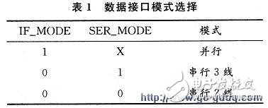
working principleThe IBIS5-B-1300 has 12 internal registers that provide the parameters and operation required for the sensor to operate. The data written to the register determines the operating state of the sensor. There are three types of data write interfaces for registers: parallel interface, serial three-wire interface, and serial two-wire interface. Different data interface modes can be selected by connecting different values ​​of the chip's IF_MODE and SER_MODE pins (as shown in Table 1).
The parallel interface uses 16 b parallel input to load new register values. The serial 3-wire interface (or serial-to-serial interface) uses the serial interface to move data into the register buffer. When the complete data word is moved into the register buffer, the data word is loaded into the register currently being encoded. Serial 2 line is a one-way interface, this article will not be analyzed.
The IBIS5-B-1300 has two shutter modes: a rolling shutter and a synchronous shutter, which are set with the bitO of the register (0000), "1" is the rolling shutter, and "0" is the synchronous shutter. The timing is shown in Figure 1, Figure 2.
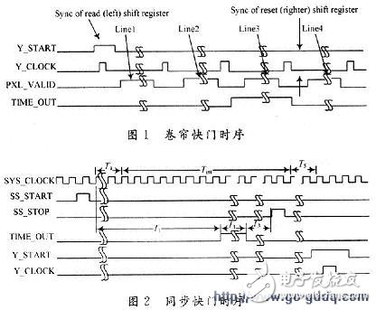
In the rolling shutter mode, the frame rate Frame period = (Nr. Lines & TImes; (RBT + Pixel Period * Nr. Pixels)).
4 Pin Automotive Connector Housing
4 Pin Automotive Connector Housing,Female 4 Pin Auto Connector,Waterproof Connector,Connector And Housing
Wenzhou Langrun Electric Co.,Ltd , https://www.langrunele.com