
When I attended DesignCon 2015 in January, I had the opportunity to hear an interesting presentation by Efficient Power Conversion CEO Alex Lidow about the development of high-power switching devices using gallium nitride (GaN) technology. I also had the privilege of encountering Steve Sandler, author of "Power Integrity - Measuring, OpTImizing, and TroubleshooTIng Power Related Parameters in Electronic Systems", he proposed Associated with measuring the Picosecond Edge speed of these devices (see the section of his article index).
Because of the higher switching speeds associated with these new power switches, we hope to see them available for switch mode power supplies and radio frequency (RF) power amplifiers. They can widely replace existing metal oxide semiconductor field effect transistors (MOSFETs) with lower "On" resistance, smaller parasitic capacitance, smaller size and faster speed. I have noticed new products using these devices. Other applications include Telecom DC-DC, Wireless Power, LiDAR and Class D Audio. It is clear that any semiconductor component switching within a few picoseconds is likely to generate a large amount of electromagnetic interference (EMI). To evaluate these GaN components, Sandler arranged for me to test some evaluation boards. One piece I chose to test was the Efficient Power Conversion Half-bridge 1MHz DC-DC Buck Converter EPC9101 (Figure 1), please refer to the other information on this test board, as well as some other reference sections.
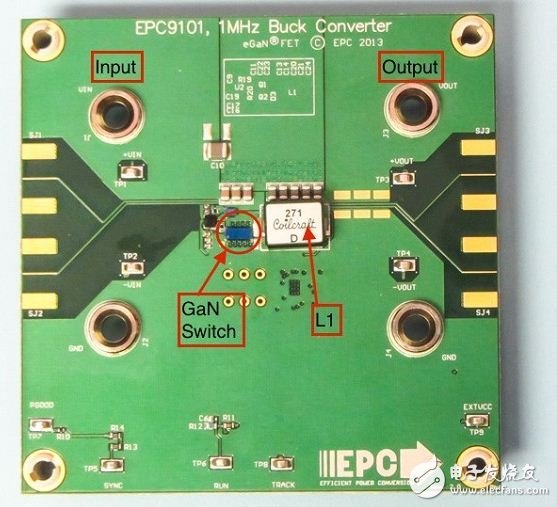
Figure 1 This demo board is used to show EMI for GaN. The GaN component is circled and I will measure the switched waveform on the left side of L1.
The demo board uses 8 to 19 volts (V) of current and converts it to 1.2 volts at 20 amps (A) (Figure 2), I let it run with 10 ohms, 2 watts (W) load, 10 volts status.
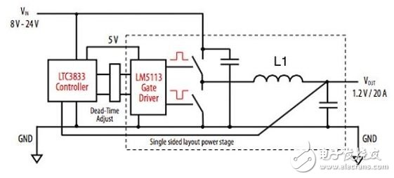
Figure 2 is a circuit diagram of a half-bridge DC-DC converter with the waveform tested at the left end of L1.
I tried to capture the edge rate with a Rohde Swartz (R&S) RT-ZS20 1.5 GHz single-ended probe (Figure 3) and detect the end of the L1 switch, but the bandwidth of the existing test equipment is so limited that it cannot be faithfully captured. . The best I can get (Figure 4) is a 1.5 nanosecond rise time (which, in terms of EMI, is quite a quick start!) To accurately record a typical 300-500 picosecond edge speed An oscilloscope with a bandwidth of 30 GHz or higher is required.
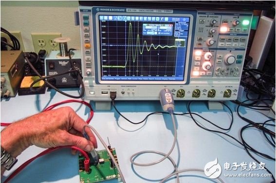
Figure 3 uses the R&S RTE1104 oscilloscope and the RT-ZS20 1.5 GHz single-ended probe to measure the leading edge.
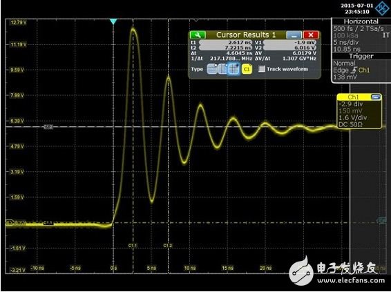
The rise time captured in Figure 4 is shown as 217MHz, which shows the fastest edge speed of 1.5 nanoseconds, but in fact, is measured under bandwidth limitations.
EMI occurrenceAlthough I couldn't capture the actual rise time, I did an evaluation reminder ringtone at 217MHz. As you will see later, when we start looking in the frequency domain, this resonance produces EMI in the bandwidth and causes a peak. Whether the signal pin and ground loop are connected to the R&S RT-ZS20 probe, the path is very short, so the reminder ringer is not caused by the probe, but the parasitic resonance of the circuit.
Next, I measured the EMI conducted on the power input cable and showed the EMI conduction characteristics through the load resistor (Figure 5).
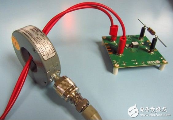
Figure 5 shows the high frequency current test with a Fischer F-33-1 current probe.
Figure 6 shows that the entire 9k~30MHz conducted emission band has very high 1MHz harmonics, and both occur at about 9MHz interval harmonics, and some of them are not sure of their original location. These harmonics are particularly high on load resistor circuits, and I suspect that without a good quality linear filter, this EMI value may fail the test of conducted radiation compliance.
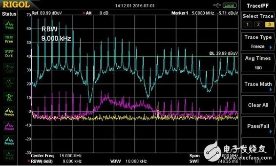
Figure 6. High-frequency current (purple line) in the power input cable measured with a Fischer F-33-1 current probe, and 10 ohm load resistance (blue line). The yellow line is an ambient noise level with a 1 MHz switching spike on top of a harmonic of approximately 9 MHz. From my experience, the level of the blue line is worrying and may cause failure of the conducted radiation test.
The bandwidth is then extended from 9KHz to 1GHz to see how far the harmonics can go, but only about 600 MHz begins to drift away. Please refer to Figure 7.
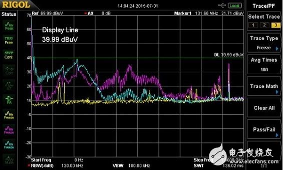
Figure 7. Conducted radiation (purple line) in the power input cable measured with a Fischer F-33-1 current probe, and 10 ohm load resistance (blue line), which is an environmental noise measurement. All of the radiation appears at 600MHz, and the resonance must be about 220MHz.
Finally, I used the R&S RS H 400-1 H-field probe (Figure 8) to measure the near field near the GaN component and the high frequency current through the load resistor (Figure 9).
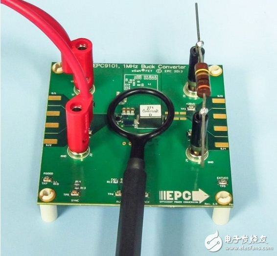
Figure 8 uses the R&S RS h400-1 H field probe to measure near-field radiation near the GaN switching device.
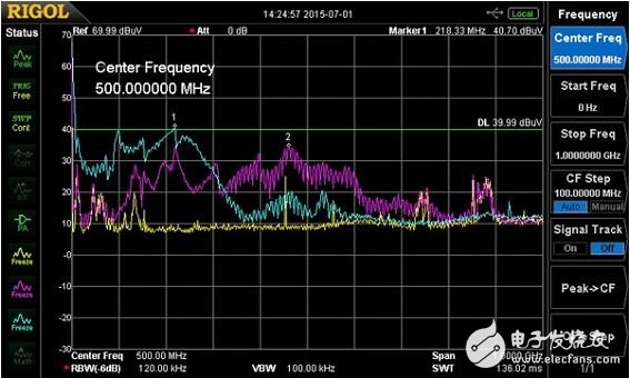
Figure 9 H field probe test results. The yellow line is the ambient noise level, the purple line is the measurement near the GaN component, and the blue line is the load resistance at 10 ohms, and the radiation is finally reduced at about 800 MHz.
Note (except for all broadband noise levels, the peak appears at approximately 220 MHz) the ringing frequency (indicator 1) and the resonance at 460 MHz (indicator 2). From past experience, I like to reduce the harmonic level to the 40dBuV Display Line, which is the green line in the screenshots above. Both resonances are quite close and thus result in a "red flag."
Significant value of GaN componentsThe value of GaN power switches is significant and the efficiency is better than MOSFETs. Although GaN technology has been around, I only see a small amount of data on how these picosecond switching devices affect product EMI. Below, I have listed some references, and when I use GaN components, I will "sweep everyone", but I believe there are more studies that need to complete the consequences of EMI, as EMI engineers and consultants will also be in the next few years. It is expected that GaN components will be used.
Android is an open source mobile operating system based on Linux platform released by Google at the end of 2007, and then improved for use in netbooks and MIDs. The platform consists of operating system, user interface and application software, and is claimed to be the first truly open and complete mobile software for mobile terminals.
To put it simply, the Android system is actually a very open system. It can not only realize the functions of the most commonly used notebook computers, but also realize various directional operations like mobile phones. Moreover, it is specially designed for mobile phones. The operating system developed for equipment has advantages in system resource consumption and human-computer interaction design. It is an operating system that combines traditional and advanced advantages.
New Android Tablet,Android Tablet,New Android Tablet
Jingjiang Gisen Technology Co.,Ltd , https://www.jsgisengroup.com