
With the continuous development of integrated circuit technology, the feature design size of integrated circuits has entered deep sub-micron, and the chip scale has expanded to one million gates. From calculations, back-end placement & routing (P&R) tools, memory usage, and operation Considering time and design timing closure, flat back-end implementations have become unbearable. In recent years, hierarchical design methods have been widely adopted to realize the back-end work of large-scale chips.
With the expansion of chip scale and the increase of design complexity, design cycle has become an issue of widespread concern. The design cycle mainly depends on 4 aspects
1. Design steps
2. The number of times each design step needs to be repeated
3. Execution time of each design step
4. Time to wait between steps
The shortening of the design cycle requires efforts from these four aspects. In addition, there is another factor that can shorten the design cycle: refer to the design process. The reference design process defines the design steps that must be performed in the design. For example, the famous rugged.script is the reference integrated process of SIS. The reference design process allows users to quickly start designing at the initial stage of the design, otherwise the designer will need to make a variety of attempts at the initial stage of the design to determine the design process.
This article first introduces IBM's application-specific integrated circuit (ASIC) design process, and then details the reusable design process (RLMREDOFLOW) for rapid physical design of sub-modules in hierarchical module design, optimized processing methods for sub-modules during top-level integration, and The advantages of the RLM design flow.
2 Introduction to the IBM ASIC design processFigure 1 describes the IBM ASIC design flow. In the initial design stage, system engineers, front-end logic design engineers, and back-end physical implementation engineers will analyze the design together, make design planning, and divide the design level according to the logic design and physical characteristics. Level division is the key factor to be considered at this stage, which will affect the strength of the optimization of the sub-module boundary during synthesis and layout, and the complexity of the connection relationship between the sub-modules. In addition, the progress of the logic design should be considered when dividing the hierarchy. If the front-end logic design of some sub-modules is earlier than other sub-modules, the physical design of this part of the sub-modules can be completed first.
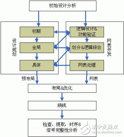
Figure 1 IBMASIC design process
3 RLM reusable design process (RLM REDO FLOW)The automated process of RLM reusable design covers all aspects of back-end design from design for test (DesignForTest, DFT), physical design to timing closure, allowing design engineers to ensure the back-end design closure through a standardized design process Flexibility and fewer iteration cycles. According to the main design nodes in the back-end design, we divide the back-end design of the entire sub-module into 9 parts for specific implementation.
1) 100 front-end processing
2) 200 to determine physical information
3) 300 prepares for timing-driven layout
4) 400 timing-driven layout
5) 500 clock insertion & clock winding
6) LateMode timing closure after 600 clock insertion
7) EarlyMode timing closure after 700 clock insertion
8) 800 detailed wiring
9) 900 delivery and acceptance
Each design step is described in detail below.
100 front-end processing
It mainly completes the generation of RLM internal test structure, including inserting the scan chain, and test logic, such as boundary scan logic, built-in self-test logic of storage devices, etc.
200 Determine physical information
Determine some of the main physical information of the RLM, including the size and shape of the RLM, the internal power supply network, the placement of the internal hard core, and the location of the port on the boundary.
1) First define the size and shape of the RLM, and the winding resources of the RLM. This is a starting point for the RLM to go down independently of the top-level design. Often the determination of this information is the result of multiple iterations, and once it is determined, it will greatly affect the reusability of the design if it needs to be modified later in the design.
2) Perform hard-core pre-layout (Floorplan) work based on the given RLM resources. Pre-layout work can be done automatically using tools or manually placed. Timing closure and winding congestion need to be taken into account. In the early design stage, it will take a lot of design time to achieve a better pre-layout result.
3) According to the pre-layout results that have been done, anti-noise treatment is performed on the areas with high port noise in the hard core.
4) Analyze the clock structure of the entire RLM.
5) For power supply design, an independent RLM power supply design requires a power loop structure on the RLM boundary to connect the power signal inside the RLM and the top layer.
6) The port placement of the RLM is completed from top to bottom, and some adjustments can be made in the subsequent design according to the requirements of the internal design of the RLM.
7) Analyze the timing of the RLM without considering the line delay to determine the rationality of the timing constraints. It should be noted that the timing constraints of the RLM boundary must be done well.
300 prepares for timing-driven layout
It mainly completes the pre-layout of the related logic of the RLM port and the internal hard core. At the same time, it can also pre-lay out other important logic according to the specific needs of the design. Through the results of the previous clock structure analysis, the clock-related logic in the design is determined, and the clock-related design will be completed independently after the layout.
400 timing-driven layout
Based on the output of the previous step, a timing-driven layout is performed on the remaining un-layout parts. And to complete the layout of the netlist for timing and physical inspection.
500 clock insertion & clock winding
According to the results of the previous clock structure analysis, the clock tree insertion work is performed on the layout design, and the clock winding is performed.
LateMode timing closure after 600 clock insertion
Call the optimization tool to optimize the setup until the setup meets the requirements
EarlyMode timing closure after 700 clock insertion
Call the optimization tool to optimize the hold until the hold meets the requirements
800 detailed wiring
Wire all signals and complete the physical characteristics inspection. Then extract parasitic parameters, noise and coupling information, perform timing analysis, and call optimization tools to optimize timing.
900 delivery and acceptance
Check the layout, timing, power consumption, noise, etc. of the RLM to ensure that the RLM design meets the acceptance requirements and can be delivered to the top layer for integration.
As can be seen from the above design process, the interaction between RLM design and top-level design is mainly in the two steps of 200 and 900. Before the RLM design process starts, the top-level designer of the chip needs to determine the location, shape (including size), port location and constraints of the RLM on the chip, the highest metal layer that can be used for RLM wiring, and the timing constraints on the RLM boundary . While RLM designers carry out RLM design, the top-level work can be carried out in parallel, and the design of each RLM can also be paralleled. The increase in parallelism greatly shortens the design cycle.
4 HATSHATS (HierarchicalAbstractTImingSignoff) is a part of IBM's hierarchical design methodology, which only extracts part of RLM information for timing analysis and optimization during top-level synthesis. In RLM, it is only the path related to the input/output ports that affects the top-level timing of the chip. The most of the timing path is from register to register. This part has already achieved timing closure in RLM. When integrated to the top level, the timing information will not change, and the timing of this part can be ignored during synthesis.
The HATS process is shown in Figure 2. After completing the RLM design, perform timing analysis and netlist analysis to remove the path from the RLM internal register to the register and the related timing constraints, extract the RLM information, and give it to the top layer for use. The extraction process is shown in Figure 3.
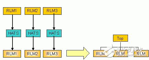
Figure 2HATS processing flow
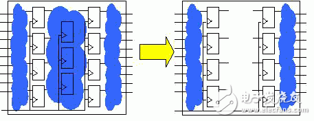
Figure 3 Extraction of RLM information
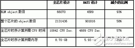
With the expansion of chip scale, the number of standard cells and hard cores has increased rapidly, and traditional design methods need to take up a lot of memory and CPU time. The HATS method eliminates redundant calculations while ensuring the quality of acceptance, greatly reducing the memory and CPU time required for chip synthesis. Table 1 shows a design example of a 90nm chip. The chip contains an RLM that has been reused 20 times. The adoption of HATS saves a lot of CPU time and memory.
Table 1 Application of HATS on chip "P"
A reusable design process is the key to shortening the design cycle. The advantages of the RLM rapid physical design method introduced in this article are summarized as follows:
1) The IBMRLM hierarchical design method has flexible and effective module division technology;
Targeted RLM division can be carried out according to customer design requirements, RLM module division can be carried out at the top level for physical design requirements that are easy to physically implement, and RLM division can be carried out comprehensively considering customer design requirements and physical design requirements.
2) Fully consider the impact of power consumption and noise on physical design;
At the initial stage of the design, a complete and reasonable power supply design is carried out, DECAP insertion, to ensure that the normal operation of the chip will not be affected by the dynamic or static voltage drop after the tape is taped out.
3) Fully consider the impact of signal integrity on chip design;
Shield critical lines, such as clock trees, to ensure that they are as accurate as possible during the acceptance phase and reduce unnecessary redundant iterations.
4) Complete timing acceptance analysis;
In the IBMRLM design process, multiple CORNER and statistical analysis are introduced. At the same time, the impact of voltage drop on the timing is fully considered at the beginning of the design, to avoid iterations due to timing issues in the acceptance stage, and to further ensure that the chip is taped out. The function in the timing is consistent with the analysis in the design phase.
5) Fully consider the boundary problem of RLM integration at the top level;
Reasonable design for the interface to ensure easy implementation of the top-level integration;
6) The design method has good flexibility;
Different engineers are allowed to work in parallel for different RLMs, and they can share and utilize a unified design script without affecting the parallel evaluation at the top level.
7) The design method is easy to update and share;
Different engineers can update the design script according to actual design needs and share it with other designers.
8) Easy to integrate;
The designed RLM can extract information to facilitate the top-level integration to quickly analyze the physical design and timing, signal integrity, power consumption and other aspects. At the same time, the internal path of the RLM can be bypassed during the top-level acceptance analysis, and the RLM can be directly flattened and flattened. analysis.
9) Easy to iterate;
After an engineer evaluates an RLM according to this method, the script required for the design is determined, and then the previous pre-layout, power supply and other information can be re-evaluated quickly according to the customer's updated ECO netlist, which reduces the time to market .
6 SummaryFor large-scale system design, a hierarchical design strategy is the direction of the industry, especially for large-scale systems that use hierarchical design to divide a large system into sub-modules, and it is easier to grasp the convergence time of small sub-module designs. Back-end engineers can work on the same design in parallel. IBM's advanced sub-module rapid design process improves the reusability of the design process and shortens the design cycle.
Hp Laptop 14-Dq 14-Fq,Hp 14-Fq Palmrest,Hp 14-Dq Palmrest,Hp 14-Fq Keyboard
S-yuan Electronic Technology Limited , https://www.syuanelectronic.com