
This article will discuss the main factors that affect SNR loss (introduced by signal scaling), how to quantify it, and more importantly: how to minimize this impact.
Many of the signals generated by sensors or systems are bipolar high voltage signals (such as the widely used ±10V signal). However, there are many simple ways to pass this signal through the ADC; various integrated high-voltage ADC solutions can also be used: this full-scale, large input signal can be processed without sacrificing SNR. These solutions require extremely high The supply voltage is sufficient to meet the input range and its power consumption is quite large (Figure 1). These high voltage ADCs also reduce the range of signal conditioning (op amp) solutions. If the signal needs to be multiplexed with the high voltage and low voltage inputs, the system cost will increase significantly (Figure 2).
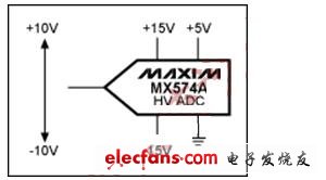
Figure 1: High-voltage ADCs can accommodate large input signals, but at the expense of higher power. To achieve this, a ±15V and +5V supply is typically required.
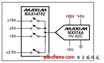
Figure 2: Multiplexed bipolar high voltage ADC system.
The input amplifier can also be used to scale the signal to match the full-scale input range of the low-voltage ADC. This signal conditioning circuit can be connected to a multiplexed input so that all signals match the range of the ADC (Figure 3).
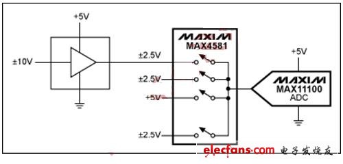
Figure 3: High voltage multiplexing system using a single low voltage ADC.
When using an amplifier for signal voltage scaling, the noise is referenced to the amplifier input. At this point, there are two main sources of noise: the input reference noise of the amplifier itself, and the reduced input reference noise of the ADC. These two noise sources are combined in a quadratic manner. In addition, the amplifier's noise is filtered by the input bandwidth of the ADC and the anti-aliasing filter between the amplifier and the ADC input, see Figure 4.
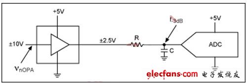
Figure 4: The scaling amplifier introduces noise, but the noise is filtered by the RC circuit and the input network of the ADC.
The calculation formula for the system SNR (amplifier input) is:
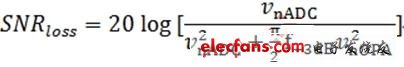
Where: VnADC is the input RMS noise of the ADC; VnOPA is the input reference noise of the amplifier (X times the input reference) = single pole -3dB frequency.
Given the full-scale range of the ADC, the input reference noise of the ADC, and the scale factor of the amplifier, there are two variables that affect the target of SNR loss reduction: the cutoff frequency of the filter and the input reference noise of the amplifier.
If the source has low frequency components, a filter can be designed to allow the amplifier to tolerate large input noise (higher input noise is usually associated with lower power and cost). If the ADC limits the bandwidth of the system, the amplifier needs to have low enough input reference noise to keep the SNR loss within an acceptable range.
For example, given a ±10V input signal and a 5VP-P full-scale ADC with a SNR of 92dB, the scaling factor (the ratio of input to full-scale range) is 4. The ADC input reference noise in the datasheet is 44.4. nV RMS . Assuming that the cutoff frequency of the filter is 10 kHz and the input reference noise of the amplifier is 10 nV / (Hz) 1/2, the loss of SNR is: SNR (loss) = 0.035 dB.
If there is no filter and the ADC bandwidth is assumed to be 10MHz, the required input reference noise becomes 0.3nV/(Hz) 1/2 in order to achieve the same SNR loss, which is very strict.
For an ADC with the same bandwidth of 10MHz, if SNR(loss)=0.5dB is allowed, the noise requirement for the amplifier is 4nV/(Hz) 1/2, which is relatively easy to implement.
Therefore, given the system bandwidth and tolerable SNR loss, adding a proportional amplifier to convert the high voltage signal to a full-scale low-voltage ADC would be a viable solution. This solution enables a cost-effective system when feeding multiple signals with different swings to a multiplexed low-voltage ADC.
ZGAR Vape Disposable Pods
ZGAR electronic cigarette uses high-tech R&D, food grade disposable pod device and high-quality raw material. All package designs are Original IP. Our designer team is from Hong Kong. We have very high requirements for product quality, flavors taste and packaging design. The E-liquid is imported, materials are food grade, and assembly plant is medical-grade dust-free workshops.
From production to packaging, the whole system of tracking, efficient and orderly process, achieving daily efficient output. WEIKA pays attention to the details of each process control. The first class dust-free production workshop has passed the GMP food and drug production standard certification, ensuring quality and safety. We choose the products with a traceability system, which can not only effectively track and trace all kinds of data, but also ensure good product quality.
We offer best price, high quality Pods, Pods Touch Screen, Empty Pod System, Pod Vape, Disposable Pod device, E-cigar, Vape Pods to all over the world.
Much Better Vaping Experience!
ZGAR Neo Vape Pods, ZGAR Disposable Vape, ZGAR Vape Pods System Vape,ZGAR Vape Pods Disposable Pod Vape Systems
Zgar International (M) SDN BHD , https://www.szvape-pods.com