
Embedded operating speed is high, the system is more complex, often integrating ultra-large-scale FPGA devices, DSP devices, DDR memory and various interface circuits. This puts higher requirements on the output voltage value, power consumption, voltage accuracy, power-up sequence and power supply integrity of the power supply.
Here we introduce a design scheme of embedded single board computer power supply based on CPCI. The design is mainly used in aviation equipment and military vehicle equipment.
2. System power demand analysis and device modeling
Figure 1 is a block diagram of the overall structure of the system. The system is composed of CPU and DDR memory connected to it, PCI interface, clock, power supply, EBC bus and external interface circuit. The CPU uses PowerPC 440EPx from AMCC.

2.1 System power requirements
The system power supply is more complex, with up to 8 different power supply voltage values, of which 5 V and 3.3 V are provided by the CPCI chassis. 5 V is supplied to the DC / DC device to step down to generate other power supply voltages, and at the same time to power the transformer of the 1553 bus. 3. 3 V is the main power supply of the system, including USB PHY, clock device, FPGA and CPU, and I / O part of PCI bridge device (PLX6466). Other power supply voltages are derived from 5V or 3.3V through the power supply device.
Tables 1 and 2 show the power consumption requirements of the CPU and PCI bridge devices, respectively. The CPU device has no requirements for the power-on sequence. Among them, VDD 1.5 V is the core voltage of PPC440EPx, SOVDD is the DDR2 interface power supply of the CPU; 1.8 V is the core voltage of the PCI bridge, and VDDIO is the interface power supply of the PCI bridge.
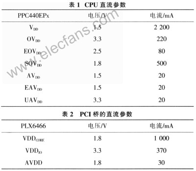
The system uses DDR2 as the memory, uses 4 Micron MT47H64M16, the capacity is 512 MB. The power supply voltage of the core, interface and DLL of each DDR2 device is 1.8 V, and the maximum current is 440 mA. In addition, pay special attention to the VREF of DDR2 and the port connected to the address and control signal voltage VTT, the voltage value of which is 0.9 V. Among them, VREF has very strict requirements on tolerance (less than 2%), but its requirements on current are relatively small. And VTT not only has strict tolerance requirements, but also requires that it can output or absorb a large current in an instant. At the same time, VREF must change with VDD, and VTT must also track changes in VREF. Ordinary LDOs are difficult to accomplish such work, and must use dedicated DDR termination power devices.
The system uses Spartan3 FPGA device XC3S200 to realize the design of 1553 transceiver and some interface circuits. The device uses three voltage core voltages VCCINT (1.2 V), auxiliary voltage VCCAUX (2.5 V) and interface voltage VCCO (3.3 V). There is a power-on reset circuit inside the FPGA. Only when all three power signals reach their respective threshold voltages, the reset signal is released. Therefore, there is no requirement for the power-up sequence of the three power signals. However, if VCCINT is powered up before VCCAUX, an additional instantaneous current of several hundred milliamperes will be added at power-up. To estimate the power consumption of FPGA devices, you can use the tool XPower EsTImator (XPE) based on a spreadsheet or call XPower directly under ISE. The system uses XPower software to estimate the power consumption requirements of the design: VCCINT is 50 mA and VCCAUX is 10 mA. The system uses two 88E1111 as the PHY device of Gigabit Ethernet. The device uses 2.5 V as the voltage (410 mA) and 1.0 V as the core voltage (250 mA). In addition to the above integrated circuits, the system also has circuits such as serial interface, USB interface, clock, etc., but the power consumption is relatively low. It can be seen from the analysis: 1.5 V and 1.8 V require the use of high-power power supply devices, DDR2 power supplies require special power supply devices, and the power requirements of other voltages are relatively small.
2. 2 power device selection
Power supply devices are mainly divided into two types: linear regulators and DC / DC converters. LDO is a linear regulator that is mainly used in applications where the input voltage is low and the output voltage difference is small. Its characteristics are: low cost, low noise, low quiescent current, and few external components, but its conversion efficiency is not very high, and the output current Generally not very big. The DC / DC converter has high conversion efficiency, large output current, and small quiescent current. However, due to the use of PWM control, the switching noise is relatively large and the cost is relatively high. Moreover, the external circuit is relatively complicated, and generally requires an external switch tube, an inductor and a capacitor. Many new types of DC / DC integrate the switch into the device. Therefore, only an external inductor and filter capacitor are needed.
According to the characteristics of the power supply device and the analysis of the power requirements of the system, both types of power supply devices are used in the system. However, in order to simplify the design, facilitate mass production and material management, the system uses only three different types of power devices, namely: LT3501, LDO devices TPS51100 and TPS74801. Among them, the 1.5 V and 1.8 V power supply circuits with large power consumption requirements are implemented by LT3501; the termination power supply and reference power supply of DDR2 are provided by the device TPS51100; the other power supplies of the system are provided by TPS74801.
3. System hardware circuit design
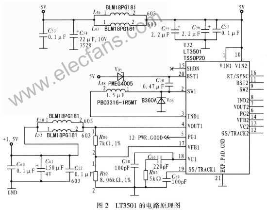
Due to the simplicity and space of the LDO circuit, the circuit design of the LT3501 is mainly discussed here. Figure 2 shows the circuit schematic of the LT3501.
3.1 Parameter configuration
3.1.1 Output voltage
The selection of the output voltage value is relatively simple, which is obtained by dividing two resistors connected between VOUT and VFR. The formula is:
![]()
In Figure 2, the voltage-dividing resistors are two resistors R680 and R682 with a precision of 1% (corresponding to R1 and R2, respectively), which is substituted into equation (1) to calculate the output voltage VOUT = 1.495 V
3.1.2 Switching frequency
The switching frequency of the LT3501 is determined by the resistance connected to the RT / SYNC pin, as shown in Figure 3. When the resistance increases from 15.4 kΩ to 133 kΩ, its switching frequency decreases from 1.5 MHz to 250 kHz. In order to reduce the size of the externally connected inductance and capacitance, and facilitate PCB design, the switching frequency is selected to be higher f = 1. 2 MHz. According to the curve shown in Figure 3, the resistance value is 20.6 kΩ.
3.1.3 Inductance value
For switching power supplies, the value of inductance is very important. According to the formula of the LT3501 data sheet:
![]()
In the formula, DC refers to the duty cycle, and its minimum value DCMIN = tON (MIN) & TImes; f = 0.24. VD is the forward voltage drop of the capture diode, and its value is about 0.4 V.
If the maximum output current requires 3 A, the inductance L can be calculated to be at least 1.2 μH from equation (2).
In order to improve efficiency and reduce output ripple, inductance is required: the effective value of the rated current should be greater than the maximum load current; at the same time, its saturation current value should be greater than 30%; the DC resistance value should be less than 0.05 Ω, and its inductance value should be greater than the theoretical value. According to this, the system chooses PB03316-1R5MT, the inductance value of this inductance is 1.5μH, the DC resistance is 0.010Ω, the effective value of the rated current is 8.0 A, and the saturation current is 6.4 A. After selecting the inductance value, it can be substituted into equation (2) to calculate the ripple current △ IL to be 0.8 A.
3.1.4 Input capacitance and output capacitance
Because the input of the switching power supply is to provide current for the output in the form of pulses, and its rise and fall times are very fast.
therefore. The input capacitor needs to be used to filter out voltage ripple to reduce EMI. And can use 4.7μF or larger X7R or X5R type capacitor bypass input signal, can also use tantalum capacitor and smaller capacity ceramic capacitor in parallel to achieve. The ceramic capacitor should be as close as possible to the input pin of the device.
The output capacitor filters the current flowing through the inductor to obtain an output voltage with little ripple. At the same time, its energy storage function can also meet the instantaneous load and stabilize the LT3501 control loop. The LT3501's control loop uses current mode, and there is no requirement for the RESR (series equivalent resistance) of the output capacitor.
Therefore, ceramic capacitors can be used as output capacitors. The value of the output capacitor can be estimated according to equation (3). Among them, MLS (Max Load Step) is the jump of the maximum current load, for example: the MLS of the system is 3A.
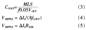
The output voltage ripple can be estimated according to equations (4) and (5): equation (4) calculates the ceramic capacitor, and equation (5) calculates the tantalum capacitor or aluminum electrolytic capacitor. The system uses X7R ceramic capacitors with good temperature characteristics in parallel with tantalum capacitors. Using equation (4), the ripple voltage is calculated to be about 0.56 mV, which satisfies the power ripple requirements of the CPU and other circuits.
3.2 PCB layout
For switching power supplies, the layout of the PCB is very important. When the switching power supply is working, there is a large step current in some branches of the circuit. This current mainly flows between the switch inside the device, the outside circulating diode and the input capacitor. The loop formed by these components should be as small as possible. In the layout, these devices, inductors and output capacitors should be laid out on the same layer of the circuit board, and the wiring should be completed on the same layer as much as possible. Under these elements, there is a continuous partial ground. The connection between the local ground and the system ground adopts a single-point connection method, and the connection point is preferably selected at the ground terminal of the output capacitor. In addition, the wiring of the SW and BST signals should be as short as possible. The LT3501 device has an exposed leadframe at the bottom, and the structure dissipates heat well. When designing the PCB. A piece of copper can be placed in the corresponding position on the bottom of the device, and connected to the large area copper of the inner layer through multiple vias.
4 Conclusion
Analyze the power consumption of the system, and design the power supply circuit of the embedded system using three kinds of power supply devices on the basis of considering certain redundancy. And use MAX705 power supply monitoring device to improve the reliability of the system. The system has been successfully verified in many practical applications and performs well.
Heated Desk Mat,Office Desk Heated Mat,Heated Keyboard Desk Mat,Warm Computer Desk Mat
Ningbo Sinco Industrial & Trading Co., Ltd. , https://www.newsinco.com