
Recently, the Institute of Microelectronics of the Chinese Academy of Sciences has successfully developed ultra-high sampling rate, wide-band 30Gsps 6bit ultra high-speed analog-to-digital converters (ADCs) and digital-to-analog converters (DACs), which has significantly shortened the technological gap with advanced countries. Releasing foreign technical barriers in this area has increased the key chips and played a significant role in promoting the development of downstream industries. What's more, the chip has already been verified for application on the 1Tb/s coherent optical OFDM transmission verification platform built by the Wuhan Institute of Posts and Telecommunications.
When the United States imposed sanctions on ZTE in March this year, ZTE’s FPGAs, optical components, and high-speed ADCs/DACs were heavily dependent on imports from the United States. Some media even believed that ZTE may face a cold winter, and even Bankruptcy. This technological breakthrough is expected to enable ZTE to shake off the unfavorable situation in ADC/DAC.
ADC chip
In the present, digital systems and analog systems have covered all aspects of life and industrial production. For example, computers are very typical digital systems. In the industrial field, many industrial inspections are continuously changing physical quantities, often with corresponding voltages and currents. The frequency or the like is simulated, and these are all analog systems. High-speed ADCs/DACs are the bridges and media for connecting digital and analog systems. Digital-to-analog converters (DACs) convert digital signals to analog signals, while analog-to-digital converters (ADCs), in turn, use analog signals. Convert to digital signal. As for how the ADC/DAC plays its role, take optical fiber communication as an example.
In optical fiber communication, since both cables and optical fiber transmit analog signals (the coaxial cable transmits analog signals, and the optical fiber transmits optical pulse signals, most of which belong to analog signals), it is necessary to convert the digital signals at the sending end first. For the analog signal, the analog signal is converted into a digital signal at the receiving end. That is, there must be a DAC at the transmitting end and an ADC at the receiving end. If the performance of the ADC/DAC chip is limited, it will directly affect the transmission rate of the optical fiber communication.
In fact, subject to the performance of the ADC/DAC chip, the current optical fiber communication does not reach the theoretical performance limit, and there is still great potential to be tapped. Therefore, high-performance ADC/DACs are used for 5G communications, as well as large data centers, Ethernet optical interconnects and short-distance interconnected communications have important implications. In addition, this technological breakthrough in the field of military microelectronics is also significant - ultra-high-speed ADC / DAC is an important radar device, in the electronic warfare, frequency agility must also rely on ultra-high-speed ADC / DAC.
Therefore, ultra-high-speed ADCs/DACs are of great significance to both national defense and civilian industries. However, such key technologies have always been dominated by developed countries such as the United States and Japan, and are very unfavorable to China. Some time ago, ZTE Communications were sanctioned by the United States. According to the media, ultra-high-speed ADCs/DACs are also listed on the sanction list.
DAC chip
In order to break the Western countries’ monopoly on ultra-high-speed ADCs/DACs, in 2006, under the leadership of Liu Xinyu, a researcher at the Institute of Microelectronics, an ultra-high-speed digital-analog hybrid circuit R&D team was established. After nearly 10 years of technology accumulation, the country’s “863†project With the support of the company, we have successfully developed an ultra-high sampling rate, wide-band 30Gsps 6-bit ADC/DAC chip. According to the information released by Microelectronics, the parameters of the 30Gsps 6-bit ADC chip and the 30Gsps 6-bit DAC chip are as follows:
The 30Gsps 6-bit ADC has an area of ​​3.9mmx3.3mm and uses 4-way interleaving technology. The sub-ADC uses an innovative and innovative folded interpolation architecture. Three error calibration circuits are integrated inside the chip, and the automatic calibration between channels can be realized through cooperation with the FPGA. The chip output uses 24 high-speed serial data interfaces and supports full-rate output at 30GSps sampling rate. The highest sampling rate of the chip is 30Gsps, which can generate 30 billion analog-to-digital conversions per second and the total power consumption is 8W. The chip's -3dB bandwidth is 18GHz. With a sampling rate of 30Gsps, the low-frequency effective bit is 5 bits, the high-frequency effective bit is greater than 3.5 bits, and the spurious-free dynamic range (SFDR) is greater than 35dBc.
The 30Gsps 6-bit DAC has a chip area of ​​3mm x 2.8mm and uses a segmented current steering DAC architecture. The chip integrates 24 high-speed serial data receivers, and 4-1MUX high-speed circuits that support full-rate output at 30GSps sampling rate. The chip also integrates a duty cycle correction and delay offset calibration circuit. The test results show that when the chip is operating at a sampling rate of 30Gsps, the low frequency spurious-free dynamic range (SFDR) reaches 44dBc, and the SFDR in the first Nyquist zone is greater than 28.5dBc. The total power consumption of the chip is 6.2W.
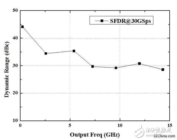
SFDR test results
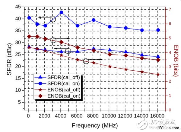
High-frequency test results
Shenzhen Linx Technology Co., Ltd. , https://www.linxheadphone.com