
The following describes the actual rectification process of a power EMI
One twenty watts of power. I will talk about my rectification through the curve of the test.
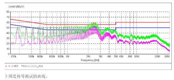
First, a curve that does not pass the test:
Above is the curve of the spatial radiation in the H direction
The above power supply is a switching power supply of about 25W. The circuit diagram of the power supply is inconvenient to upload because of customer's reasons, but we can explain it to you first. This circuit uses a 0.1uF X capacitor and a 30mH common mode inductor. The secondary output adds a 50uH I-shaped inductor. The customer's rectification requires the rectification program to produce energy.
I first looked at the product after I got the product and discovered that the MOSFETs and the heat sinks of the bidirectional diodes were not connected to the heat. (ie, the negative side of the electrolytic capacitor on the primary side of the power supply. The transformer has a layer of coiled shield and is connected to the hot ground.
My rectification plan is as follows:
It can be seen that the differential mode capacitance X is too small from the case of the 1 MHz before the conduction curve exceeds the standard, so the X capacitance is changed to 0.22 uF. And between 1-5MHz is also exceeded, so increase the common-mode inductance to 50mH, this frequency exceeding the standard is mainly caused by the leakage inductance of the transformer. A shielded copper foil was added to the outside of the transformer and it was connected to hot ground. (At the same time, a transformer was used to remove the shielding layer inside the original transformer, which changed the winding method of the transformer, and the transformer was shielded and connected to the hot ground for backup)
At the same time, the heat sinks of the MOS tube and bidirectional diode are also connected to the hot ground. At the same time, a 101/1KV capacitor was added between the D and S pins of the MOS tube. After the above rectification program, a test was performed. See the curve below:
This picture shows the transformer used on the customer's original board. I only added a shield on the outside. The test can pass but the margin is only 1dB. Obviously, it can guarantee the uncertainty caused by mass production.
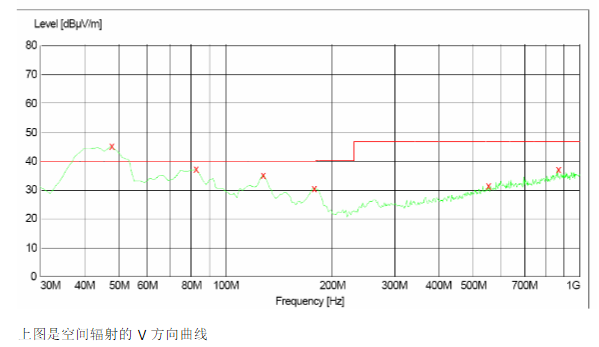
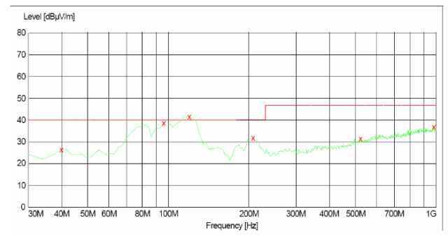
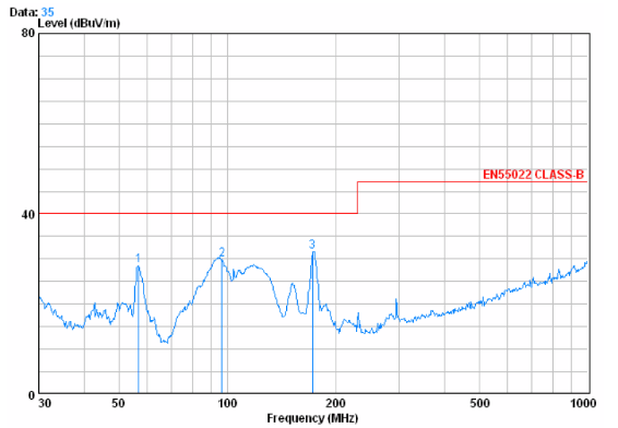
The following figure shows the direction of the curve V of the space radiation, but the margin is also small.
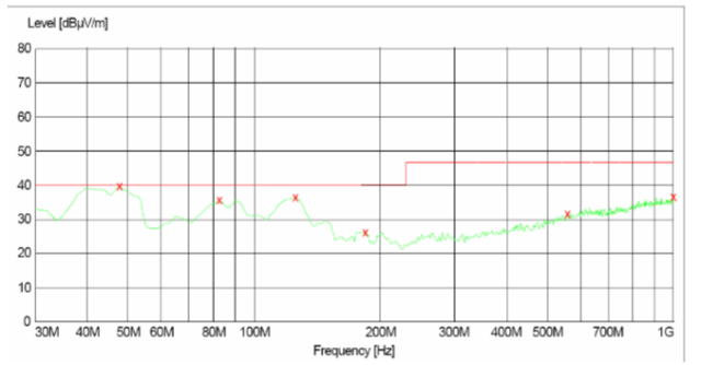
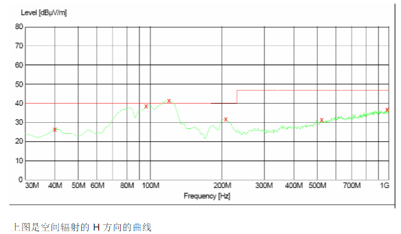
The following figure shows the curve in the H direction. It can be seen that the 100-120 MHz segment still exceeds the standard.
Based on the above situation, I made a second modification to update the transformer to the transformer that I mentioned earlier and changed the winding method. Use my spectrum analyzer to revisit the position of a product's transformer and the position of the MOS tube. Found MOS tube position curve is not a bit high, and into a regular waveform
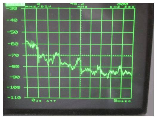
Then use the spectrum to contact the three legs of G, D, S of the MOS tube to see which foot is the radiation source and find that the radiation source of the D-pole is the largest. So I strung a string of universal inserts on the D pole. (¢3.5*8) Look at the spectrum curve of the MOS tube as follows:
As you can see at this time, the radiation of the MOS tube is significantly reduced and more stable. Then the second test was done. The results are as follows:
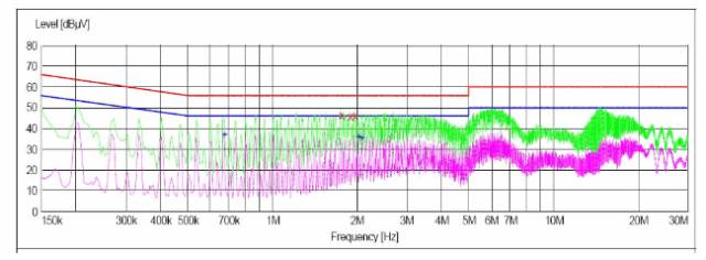
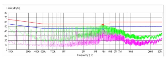
From the above figure, we can see that the conduction at this time has been very good, with the smallest amount being 8.6 dB.
The above figure shows the minimum margin of the spatial radiation curve in the V direction is 8.3 dB.
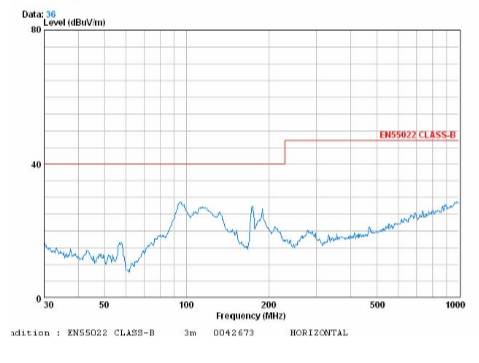
The figure above shows that the curve margin in the H direction is larger.
After two modifications, the product smoothly meets the standard test of the customer's requirements.
The final rectification plan is:
1. Connect the MOS tube and the heat sink surface of the bidirectional diode to the thermal ground of the power supply.
2. Change the X capacitance to 0.22uF.
3. Change the common mode inductance to 50mH.
4. Insert the magnetic beads of a plug in the front of the D-line circuit of the MOS tube. To eliminate the 101 capacitors connected between D and S.
5. Change the winding method of the transformer, cancel the internal shielding, and add a shielding layer on the outside. And access to hot spots.
Summary:
In fact, EMC's rectification is mainly due to the rectification of the power supply because any product must have a power source to supply power, and there is no good treatment here that will affect other places. Irrespective of the product, its radiation or conduction is mainly caused by the sensitive components inside the product. The main sensitive components for power supply products are transformers, MOS transistors, and diodes. Therefore, as long as the solution to these three aspects of coordination issues EMC is not difficult to get. The general approach to solving the EMC is to eliminate the source of interference, remove the pathway of dry conduction, and ease the source of interference.
a. Elimination is the loss of the source of interference by means of thermal energy, this is the cost of the way.
b. The way to cut off the interference conduction is to cut off the path of the interference and make it unable to interfere with the outside, that is, we often do filtering, shielding and other methods.
c. Easing the source of interference This is the way to introduce the interference source to components that are not sensitive, such as bypassing, borrowing, and grounding.
5V Power Adapter,Adapter 5V,Dc 5V Power Adapter,Switching Adapter 5V
ShenZhen Yinghuiyuan Electronics Co.,Ltd , https://www.yhypoweradapter.com